#crystal structure
Text

Advanced nuclear magnetic resonance technique reveals precise structural, dynamical details in zeolites
Zeolites are widely used in many industries, yet their intrinsic catalytic nature is not completely understood, due to the complexity of the hydroxyl-aluminum moieties.
Atomic-scale analysis of local environments for the hydroxyl species is essential for revealing the intrinsic catalytic activity of zeolites and guiding the design of high-performance catalysts. However, many unfavorable factors prohibit the elucidation of their fine structures such as low quantity, meta-stable property, structural similarity, hydrogen-bonding environment, and long-range disordered nature.
Recently, a research team led by Prof. Hou Guangjin and Prof. Chen Kuizhi from the Dalian Institute of Chemical Physics (DICP) of the Chinese Academy of Sciences (CAS) unraveled the precise structure of complex hydroxyl groups in zeolites with a comprehensive set of self-developed coupling-edited 1H-17O solid-state nuclear magnetic resonance (NMR) methods. The study was published in the Journal of the American Chemical Society.
Read more.
#Materials Science#Science#Zeolites#Crystal structure#Catalysts#Materials characterization#Nuclear magnetic resonance#NMR
11 notes
·
View notes
Text
Miller Indices and Lattice Planes
Have you ever wondered how scientists talk about the microscopic building blocks of materials? Enter the world of Miller indices and lattice levels, a language that reveals the secrets of atomic arrangements within crystals. Imagine visualizing levels of atoms stacked like bricks, each level described by a unique set of numbers that reveal its orientation and spacing.
How to determine Miller Indices?
Imagine the crystal lattice with three axes: These axes represent the basic building blocks of the crystal's structure. In a cubic crystal, for example, the axes are all perpendicular to each other and of equal length.
Identify a plane: This plane can cut through the lattice in any direction, intersecting the axes at different points.
Find the intercepts: For each axis, measure the distance from the origin to the point where the plane intersects it. If the plane doesn't intersect an axis, then the intercept is considered to be "at infinity" and is represented by a zero.
Take the reciprocals: For each non-zero intercept, take the reciprocal (flip it over).
Simplify and normalize: If any of the reciprocals have a common factor, divide them all by that factor to get the smallest possible integers.
Put the numbers together: The resulting three integers, enclosed in parentheses (h k l), are the Miller indices for that plane.
Read more:
#science#materials science#materials#materials science and engineering#alloys#metals#mechanical properties#mechanical properties of materials#crystal structure#crystalline
2 notes
·
View notes
Photo

#https://en.wikipedia.org/wiki/Illite_crystallinity#wikipedia#crystal structure#mica#illite#chemistry
2 notes
·
View notes
Text
Propelling atomically layered magnets toward green computers
New Post has been published on https://thedigitalinsider.com/propelling-atomically-layered-magnets-toward-green-computers/
Propelling atomically layered magnets toward green computers
Globally, computation is booming at an unprecedented rate, fueled by the boons of artificial intelligence. With this, the staggering energy demand of the world’s computing infrastructure has become a major concern, and the development of computing devices that are far more energy-efficient is a leading challenge for the scientific community.
Use of magnetic materials to build computing devices like memories and processors has emerged as a promising avenue for creating “beyond-CMOS” computers, which would use far less energy compared to traditional computers. Magnetization switching in magnets can be used in computation the same way that a transistor switches from open or closed to represent the 0s and 1s of binary code.
While much of the research along this direction has focused on using bulk magnetic materials, a new class of magnetic materials — called two-dimensional van der Waals magnets — provides superior properties that can improve the scalability and energy efficiency of magnetic devices to make them commercially viable.
Although the benefits of shifting to 2D magnetic materials are evident, their practical induction into computers has been hindered by some fundamental challenges. Until recently, 2D magnetic materials could operate only at very low temperatures, much like superconductors. So bringing their operating temperatures above room temperature has remained a primary goal. Additionally, for use in computers, it is important that they can be controlled electrically, without the need for magnetic fields. Bridging this fundamental gap, where 2D magnetic materials can be electrically switched above room temperature without any magnetic fields, could potentially catapult the translation of 2D magnets into the next generation of “green” computers.
A team of MIT researchers has now achieved this critical milestone by designing a “van der Waals atomically layered heterostructure” device where a 2D van der Waals magnet, iron gallium telluride, is interfaced with another 2D material, tungsten ditelluride. In an open-access paper published March 15 in Science Advances, the team shows that the magnet can be toggled between the 0 and 1 states simply by applying pulses of electrical current across their two-layer device.
Play video
The Future of Spintronics: Manipulating Spins in Atomic Layers without External Magnetic Fields
Video: Deblina Sarkar
“Our device enables robust magnetization switching without the need for an external magnetic field, opening up unprecedented opportunities for ultra-low power and environmentally sustainable computing technology for big data and AI,” says lead author Deblina Sarkar, the AT&T Career Development Assistant Professor at the MIT Media Lab and Center for Neurobiological Engineering, and head of the Nano-Cybernetic Biotrek research group. “Moreover, the atomically layered structure of our device provides unique capabilities including improved interface and possibilities of gate voltage tunability, as well as flexible and transparent spintronic technologies.”
Sarkar is joined on the paper by first author Shivam Kajale, a graduate student in Sarkar’s research group at the Media Lab; Thanh Nguyen, a graduate student in the Department of Nuclear Science and Engineering (NSE); Nguyen Tuan Hung, an MIT visiting scholar in NSE and an assistant professor at Tohoku University in Japan; and Mingda Li, associate professor of NSE.
Breaking the mirror symmetries
When electric current flows through heavy metals like platinum or tantalum, the electrons get segregated in the materials based on their spin component, a phenomenon called the spin Hall effect, says Kajale. The way this segregation happens depends on the material, and particularly its symmetries.
“The conversion of electric current to spin currents in heavy metals lies at the heart of controlling magnets electrically,” Kajale notes. “The microscopic structure of conventionally used materials, like platinum, have a kind of mirror symmetry, which restricts the spin currents only to in-plane spin polarization.”
Kajale explains that two mirror symmetries must be broken to produce an “out-of-plane” spin component that can be transferred to a magnetic layer to induce field-free switching. “Electrical current can ‘break’ the mirror symmetry along one plane in platinum, but its crystal structure prevents the mirror symmetry from being broken in a second plane.”
In their earlier experiments, the researchers used a small magnetic field to break the second mirror plane. To get rid of the need for a magnetic nudge, Kajale and Sarkar and colleagues looked instead for a material with a structure that could break the second mirror plane without outside help. This led them to another 2D material, tungsten ditelluride. The tungsten ditelluride that the researchers used has an orthorhombic crystal structure. The material itself has one broken mirror plane. Thus, by applying current along its low-symmetry axis (parallel to the broken mirror plane), the resulting spin current has an out-of-plane spin component that can directly induce switching in the ultra-thin magnet interfaced with the tungsten ditelluride.
“Because it’s also a 2D van der Waals material, it can also ensure that when we stack the two materials together, we get pristine interfaces and a good flow of electron spins between the materials,” says Kajale.
Becoming more energy-efficient
Computer memory and processors built from magnetic materials use less energy than traditional silicon-based devices. And the van der Waals magnets can offer higher energy efficiency and better scalability compared to bulk magnetic material, the researchers note.
The electrical current density used for switching the magnet translates to how much energy is dissipated during switching. A lower density means a much more energy-efficient material. “The new design has one of the lowest current densities in van der Waals magnetic materials,” Kajale says. “This new design has an order of magnitude lower in terms of the switching current required in bulk materials. This translates to something like two orders of magnitude improvement in energy efficiency.”
The research team is now looking at similar low-symmetry van der Waals materials to see if they can reduce current density even further. They are also hoping to collaborate with other researchers to find ways to manufacture the 2D magnetic switch devices at commercial scale.
This work was carried out, in part, using the facilities at MIT.nano. It was funded by the Media Lab, the U.S. National Science Foundation, and the U.S. Department of Energy.
#ai#amp#artificial#Artificial Intelligence#atomic#Big Data#binary#career#career development#challenge#code#collaborate#Community#computation#computer#computer memory#Computer science and technology#computers#computing#crystal#crystal structure#data#Design#development#devices#direction#efficiency#electron#Electronics#electrons
0 notes
Text
For example, we have observed unprecedented spin crossover behaviour in a dicobalt complex (figure 13.44), and more recently we have determined the crystal structure of an unused mixed spin state diiron complex (figure 13.45).
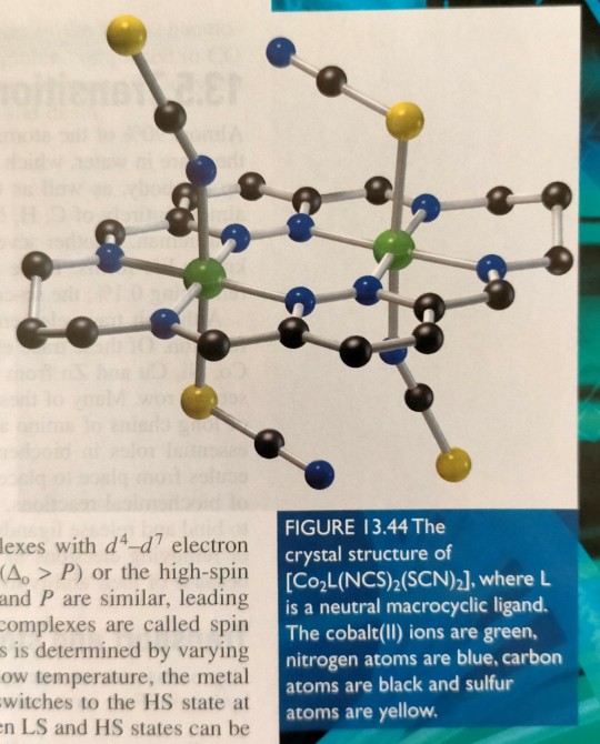
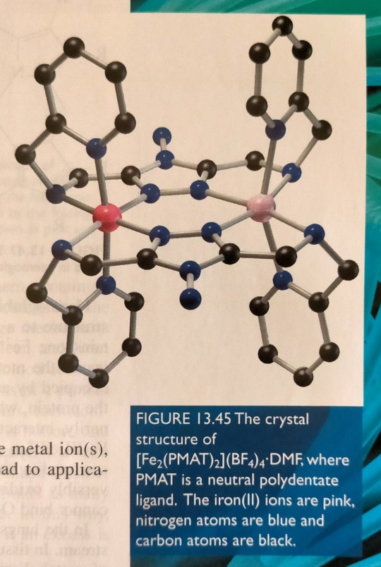
"Chemistry" 2e - Blackman, A., Bottle, S., Schmid, S., Mocerino, M., Wille, U.
#book quotes#chemistry#nonfiction#textbook#spin#electrons#electron configuration#crystal structure#cobalt#iron#nitrogen#carbon#sulfur
1 note
·
View note
Text
These crystal structures can be described such that all the atoms in a unit cell are associated with the lattice points, i.e. the number of atoms in the unit cell and the number of lattice points will be identical.
"Chemistry" 2e - Blackman, A., Bottle, S., Schmid, S., Mocerino, M., Wille, U.
0 notes
Text
good fucking lord we need to demystify minerals. crystals do not have healing or magical powers you guys are just getting scammed
42K notes
·
View notes
Text
X-Ray Diffraction
Introduction
X-ray diffraction (XRD) is a powerful technique used for the study of crystalline materials. By analyzing the way in which a beam of X-rays diffracts off a crystalline sample, one can determine the atomic and molecular structure of the material, including bond lengths and angles, atomic positions, and overall symmetry.
The Principle of XRD
The principle behind X-ray diffraction is…
View On WordPress
0 notes
Text
Crystal Gregory, Embody 2, (handwoven cast in concrete), 2023 [© Crystal Gregory]


250 notes
·
View notes
Note

just realized i draw the angels' faces like little snowflakes
yesss yayyy
86 notes
·
View notes
Photo


Lightwarden AU
He takes so little, and so sparingly. To refrain from consuming living aether, to go against his, eater's, very point of existence... Frivolus may appear docile and passive, but Exarch only dares to imagine the amount of strength that goes into his perpetual inner battle. Sacrifice. Self-destruction in the name of love. Oh, how he wishes to stay oblivious to this evil irony.
#i came up with an actual structure for the au story#with a proper beginning and end#the end isn't even THAT horrible mind you#now i've just gotta find the time and energy to properly present it in text and visuals#shb spoilers#ffxiv#vivien rell#frivolus#crystal exarch#g'raha tia#wol x g'raha tia#wolgraha#lightwarden#lightwarden au#own: next lvl
481 notes
·
View notes
Text

Revolutionary X-ray microscope unveils sound waves deep within crystals
Researchers at the Department of Energy's SLAC National Accelerator Laboratory. Stanford University, and Denmark Technical University have designed a cutting-edge X-ray microscope capable of directly observing sound waves at the tiniest of scales—the lattice level within a crystal. These findings, published last week in Proceedings of the National Academy of Sciences, could change the way scientists study ultrafast changes in materials and the resulting properties.
"The atomic structure of crystalline materials gives rise to their properties and associated 'use-case' for an application," said one of the researchers, Leora Dresselhaus-Marais, an assistant professor at Stanford and SLAC.
"The crystalline defects and atomic scale displacements describe why some materials strengthen while others shatter in response to the same force. Blacksmiths and semiconductor manufacturing have perfected our ability to control some types of defects, however, few techniques today can image these dynamics in real-time at the appropriate scales to resolve how those the distortions connect to the bulk properties."
Read more.
#Materials Science#Science#X Rays#Microscopy#Sound#Crystal structure#Defects#Materials characterization
22 notes
·
View notes
Text
Crystalline imperfections of materials
In reality, crystals are never perfect, and they contain various types of imperfections and defects that affect many of their physical and mechanical properties, which in turn affect many important engineering properties of materials such asthe cold formability of alloys, the electronic conductivity of semiconductors, the rate of migration of atoms in alloys (Diffusion), and the corrosion of metals.
Crystalline Imperfections
Crystalline imperfections, also known as crystal defects or lattice defects, are deviations from the ideal atomic arrangement in a crystalline material. Crystalline materials have a regular and repeating three-dimensional atomic or molecular structure. However, in reality, perfect crystals are rare, and most materials contain various types of imperfections. These imperfections can significantly impact the properties and behavior of the material.
Types of imperfections in crystals
Crystalline imperfections are classified according to their geometry and shape into:
Zero-dimensional or point defects.
One-dimensional or line defects (dislocations).
Two-dimensional or Planar defects.
Three-dimensional volume defects.
Read more:
#science#materials science#engineering#materials science and engineering#mechanical properties of materials#defects#Imperfections#crystalline defects#crystal structure#Crystalline imperfections of materials
0 notes
Text
one of the biggest questions i feel folks on tumblr are always trying to answer is "how do i be better? how do i get to the next level of witchcraft? how do i access advanced stuff?" and the thing is, babes, is that that shit isn't external.
you become an "advanced witch" when you stop categorising topics as beginner or intermediate or advanced! there are no rules.
a lot of people make an effort to warn so-called "baby witches" away from different types of magick - "don't do love magick or hexing ever! don't contact X deity until you've been practicing for a year! you have to have been practicing for at least a month to do a spell!" - why? what does that achieve, apart from perpetuating fear mongering and policing others religion?
it comes from this idea that there's a right way to practice, and more importantly, that if you fuck something up then that's sacrilege. if you give a deity the wrong offering they'll be angry with you (and that's the end of that relationship). if you do a love spell without considering the effects then you'll do irreparable damage and be shamed!! you must follow these ideas, that crystals and tarot and candles (conveniently all the things that require you to spend money) are "beginner-friendly" and everything that our ancestors would have done is too advanced for you.
whatever experience you're on is personal to you. no-one knows more than you about your practice than you. if you wanna do a hex, some post on tumblr shouldn't going to stop you. if you fuck it up, you'll learn!
and frankly, witchblr would be a better place if we stopped looking at everything as a strict guide to follow, and as a place where we all share what our practice looks like, and approach each other with curiosity instead of pride and superiority.
#you are not better because you have never hexed anyone#and you are not worse because you have#you are not better because you have fifty million crystals#or because you work with a deity#witchcraft is not a goddamn competition#and it isnt an organised structured religion#there is no sin or virtue#there is just being#witchblr#wicca#pagan#hearth witch#folk witch#witchcraft#divination#tarot#astrology#paganism
66 notes
·
View notes
Text
Study Unlocks Nanoscale Secrets for Designing Next-Generation Solar Cells - Technology Org
New Post has been published on https://thedigitalinsider.com/study-unlocks-nanoscale-secrets-for-designing-next-generation-solar-cells-technology-org/
Study Unlocks Nanoscale Secrets for Designing Next-Generation Solar Cells - Technology Org
Perovskites, a broad class of compounds with a particular kind of crystal structure, have long been seen as a promising alternative or supplement to today’s silicon or cadmium telluride solar panels. They could be far more lightweight and inexpensive and could be coated onto virtually any substrate, including paper or flexible plastic that could be rolled up for easy transport.
A team of MIT researchers and several other institutions has revealed ways to optimize efficiency and better control degradation, by engineering the nanoscale structure of perovskite devices. Team members include Madeleine Laitz, left, and lead author Dane deQuilettes. Illustration by the researchers / MIT
In their efficiency at converting sunlight to electricity, perovskites are becoming comparable to silicon, whose manufacture still requires long, complex, and energy-intensive processes. One big remaining drawback is longevity: They tend to break down in a matter of months to years, while silicon solar panels can last more than two decades. And their efficiency over large module areas still lags behind silicon. Now, a team of researchers at MIT and several other institutions has revealed ways to optimize efficiency and better control degradation by engineering the nanoscale structure of perovskite devices.
The study reveals new insights on how to make high-efficiency perovskite solar cells, and also provides new directions for engineers working to bring these solar cells to the commercial marketplace. The work is described in the journal Nature Energy in a paper by Dane deQuilettes, a recent MIT postdoc who is now co-founder and chief science officer of the MIT spinout Optigon, along with MIT professors Vladimir Bulovic and Moungi Bawendi, and 10 others at MIT and in Washington state, the U.K., and Korea.
“Ten years ago, if you had asked us what would be the ultimate solution to the rapid development of solar technologies, the answer would have been something that works as well as silicon but whose manufacturing is much simpler,” Bulovic says. “And before we knew it, the field of perovskite photovoltaics appeared. They were as efficient as silicon, and they were as easy to paint on as it is to paint on a piece of paper. The result was tremendous excitement in the field.”
Nonetheless, “there are some significant technical challenges of handling and managing this material in ways we’ve never done before,” he says. But the promise is so great that many hundreds of researchers around the world have been working on this technology. The new study looks at a very small but key detail: how to “passivate” the material’s surface, changing its properties so that the perovskite no longer degrades so rapidly or loses efficiency.
“The key is identifying the chemistry of the interfaces, the place where the perovskite meets other materials,” Bulovic says, referring to the places where different materials are stacked next to perovskite in order to facilitate the flow of current through the device.
Engineers have developed methods for passivation, for example by using a solution that creates a thin passivating coating. But they’ve lacked a detailed understanding of how this process works — which is essential to make further progress in finding better coatings. The new study “addressed the ability to passivate those interfaces and elucidate the physics and science behind why this passivation works as well as it does,” Bulovic says.
The team used some of the most powerful instruments available at laboratories around the world to observe the interfaces between the perovskite layer and other materials, and how they develop, in unprecedented detail. This close examination of the passivation coating process and its effects resulted in “the clearest roadmap as of yet of what we can do to fine-tune the energy alignment at the interfaces of perovskites and neighboring materials,” and thus improve their overall performance, Bulovic says.
While the bulk of a perovskite material is in the form of a perfectly ordered crystalline lattice of atoms, this order breaks down at the surface. There may be extra atoms sticking out or vacancies where atoms are missing, and these defects cause losses in the material’s efficiency. That’s where the need for passivation comes in.
“This paper is essentially revealing a guidebook for how to tune surfaces, where a lot of these defects are, to make sure that energy is not lost at surfaces,” deQuilettes says. “It’s a really big discovery for the field,” he says. “This is the first paper that demonstrates how to control and engineer surface fields in perovskites systematically.”
The common passivation method is to bathe the surface in a solution of a salt called hexylammonium bromide, a technique developed at MIT several years ago by Jason Jungwan Yoo PhD ’20, who is a co-author of this paper, that led to multiple new world-record efficiencies. By doing that “you form a very thin layer on top of your defective surface, and that thin layer actually passivates a lot of the defects really well,” deQuilettes says. “And then the bromine, which is part of the salt, actually penetrates into the three-dimensional layer in a controllable way.” That penetration helps to prevent electrons from losing energy to defects at the surface.
These two effects, produced by a single processing step, produces the two beneficial changes simultaneously. “It’s really beautiful because usually you need to do that in two steps,” deQuilettes says.
The passivation reduces the energy loss of electrons at the surface after they have been knocked loose by sunlight. These losses reduce the overall efficiency of the conversion of sunlight to electricity, so reducing the losses boosts the net efficiency of the cells.
He says That could rapidly improve the materials’ efficiency in converting sunlight to electricity. The recent efficiency records for a single perovskite layer, several of them set at MIT, have ranged from about 24 to 26 percent, while the maximum theoretical efficiency that could be reached is about 30 percent, according to deQuilettes.
An increase of a few percent may not sound like much, but in the solar photovoltaic industry such improvements are highly sought after. “In the silicon photovoltaic industry, if you’re gaining half of a percent in efficiency, that’s worth hundreds of millions of dollars on the global market,” he says. A recent shift in silicon cell design, essentially adding a thin passivating layer and changing the doping profile, provides an efficiency gain of about half of a percent. As a result, “the whole industry is shifting and rapidly trying to push to get there.” The overall efficiency of silicon solar cells has only seen very small incremental improvements for the last 30 years, he says.
The record efficiencies for perovskites have mostly been set in controlled laboratory settings with small postage-stamp-size samples of the material. “Translating a record efficiency to commercial scale takes a long time,” deQuilettes says. “Another big hope is that with this understanding, people will be able to engineer large areas better to have these passivating effects.”
There are hundreds of different kinds of passivating salts and many different kinds of perovskites, so the basic understanding of the passivation process provided by this new work could help guide researchers to find even better combinations of materials, the researchers suggest. “There are so many different ways you could engineer the materials,” he says.
“I think we are on the doorstep of the first practical demonstrations of perovskites in the commercial applications,” Bulovic says. “And those first applications will be a far cry from what we’ll be able to do a few years from now.” He adds that perovskites “should not be seen as a displacement of silicon photovoltaics. It should be seen as an augmentation — yet another way to bring about more rapid deployment of solar electricity.”
“A lot of progress has been made in the last two years on finding surface treatments that improve perovskite solar cells,” says Michael McGehee, a professor of chemical engineering at the University of Colorado who was not associated with this research. “A lot of the research has been empirical with the mechanisms behind the improvements not being fully understood. This detailed study shows that treatments can not only passivate defects, but can also create a surface field that repels carriers that should be collected at the other side of the device. This understanding might help further improve the interfaces.”
Written by David L. Chandler
Source: Massachusetts Institute of Technology
You can offer your link to a page which is relevant to the topic of this post.
#applications#atoms#cadmium#cell#Cells#chemical#Chemical engineering#chemistry#Chemistry & materials science news#coatings#crystal#crystal structure#crystalline#deployment#Design#development#devices#easy#effects#efficiency#electricity#electrons#energy#Energy & fuel news#Engineer#engineering#engineers#form#Fundamental physics news#Global
0 notes
Text
Figure 16.9A illustrates several of the structural domains in phytochrome. (...) A comparison of the domain structures of plant phytochrome with the prokaryotic phytochromes Cph1 (cyanobacterial phytochrome 1) and BphPs (bacterial phytochrome-like proteins) highlights several differences between plant and prokaryotic phytochromes, including the absence of two PRD domains and the presence of the HKRD domain in place of a functional histidine kinase domain of prokaryotes (see Figure 16.9A). (...) The crystal structure of the light-sensing N-terminal half of Arabidopsis phyB is shown in Figure 16.9B. (...) Based on studies with the bacterial phytochrome of Deinococcus radiodurans and Arabidopsis phytochrome, a toggle model has been proposed for phytochrome interconversion, as illustrated in Figure 16.9C.

"Plant Physiology and Development" int'l 6e - Taiz, L., Zeiger, E., Møller, I.M., Murphy, A.
#book quotes#plant physiology and development#nonfiction#textbook#phytochrome#crystal structure#arabidopsis#deinococcus#deinococcus radiodurans#toggle model#red light#far red light#prokaryote#prd#pas related domain#hkrd#histidine kinase related domain
1 note
·
View note
Last Seen Blogs

babs74
Babs74

plantias
Plantias
plantias
Plantias

swiftlovinggay
A Mess

countdown-til-sanders-take-over
Let's see how powerful the countdowns are