#computer chips
Photo

BYTE November 1994
An assortment of new CPUs featured on this issue’s cover, with the editorial insisting they hadn’t become interchangeable commodities yet (although the “significance of the Intel/HP alliance” was that it might “spell the beginning of the end for RISC,” as in the PowerPC). Along with reviews of “Internet guides,” one article discussed how companies were beginning to establish themselves on the World Wide Web, with successors to Mosaic already on the horizon.
89 notes
·
View notes
Text
A first-ever complete map for elastic strain engineering - Technology Org
New Post has been published on https://thedigitalinsider.com/a-first-ever-complete-map-for-elastic-strain-engineering-technology-org/
A first-ever complete map for elastic strain engineering - Technology Org
New research by a team of MIT engineers offers a guide for fine-tuning specific material properties.
Without a map, it can be impossible to know not only where you are but also where you’re going, and that’s especially true when it comes to materials’ properties.
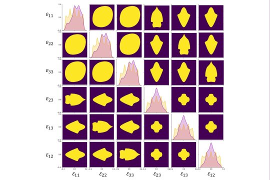
The “map,” or the phonon stability boundary, is a graphical representation that plots the stability regions of a crystal as a function of strain. This map helps scientists and engineers determine the conditions under which a material can exist in a particular phase and when it might fail or transition to another phase. By analyzing the phonon stability boundary, researchers can understand material properties at extreme conditions and design new materials with desired characteristics. Image courtesy of the researchers / MIT
For decades, scientists have understood that while bulk materials behave in certain ways, those rules can break down for materials at the micro- and nano-scales, and often in surprising ways. One of those surprises was the finding that, for some materials, applying even modest strains — a concept known as elastic strain engineering — on materials can dramatically improve certain properties, provided those strains stay elastic and do not relax away by plasticity, fracture, or phase transformations. Micro- and nano-scale materials are especially good at holding applied strains in the elastic form.
Precisely how to apply those elastic strains (or equivalently, residual stress) to achieve certain material properties, however, had been less clear — until recently.
Using a combination of first principles calculations and machine learning, a team of MIT researchers has developed the first-ever map of how to tune crystalline materials to produce specific thermal and electronic properties.
Led by Ju Li, the Battelle Energy Alliance Professor in Nuclear Engineering and professor of materials science and engineering, the team described a framework for understanding precisely how changing the elastic strains on a material can fine-tune properties like thermal and electrical conductivity. The work is described in an open-access paper published in PNAS.
“For the first time, by using machine learning, we’ve been able to delineate the complete six-dimensional boundary of ideal strength, which is the upper limit to elastic strain engineering, and create a map for these electronic and phononic properties,” Li says. “We can now use this approach to explore many other materials. Traditionally, people create new materials by changing the chemistry.”
“For example, with a ternary alloy, you can change the percentage of two elements, so you have two degrees of freedom,” he continues. “What we’ve shown is that diamond, with just one element, is equivalent to a six-component alloy, because you have six degrees of elastic strain freedom you can tune independently.”
Small strains, big material benefits
The paper builds on a foundation laid as far back as the 1980s, when researchers first discovered that the performance of semiconductor materials doubled when a small — just 1 percent — elastic strain was applied to the material.
While that discovery was quickly commercialized by the semiconductor industry and today is used to increase the performance of microchips in everything from laptops to cellphones, that level of strain is very small compared to what we can achieve now, says Subra Suresh, the Vannevar Bush Professor of Engineering Emeritus.
In a 2018 Science paper, Suresh, Dao, and colleagues demonstrated that 1 percent strain was just the tip of the iceberg.
As part of a 2018 study, Suresh and colleagues demonstrated for the first time that diamond nanoneedles could withstand elastic strains of as much as 9 percent and still return to their original state. Later on, several groups independently confirmed that microscale diamond can indeed elastically deform by approximately 7 percent in tension reversibly.
“Once we showed we could bend nanoscale diamonds and create strains on the order of 9 or 10 percent, the question was, what do you do with it,” Suresh says. “It turns out diamond is a very good semiconductor material … and one of our questions was, if we can mechanically strain diamond, can we reduce the band gap from 5.6 electron-volts to two or three? Or can we get it all the way down to zero, where it begins to conduct like a metal?”
To answer those questions, the team first turned to machine learning in an effort to get a more precise picture of exactly how strain altered material properties.
“Strain is a big space,” Li explains. “You can have tensile strain, you can have shear strain in multiple directions, so it’s a six-dimensional space, and the phonon band is three-dimensional, so in total there are nine tunable parameters. So, we’re using machine learning, for the first time, to create a complete map for navigating the electronic and phononic properties and identify the boundaries.”
Armed with that map, the team subsequently demonstrated how strain could be used to dramatically alter diamond’s semiconductor properties.
“Diamond is like the Mt. Everest of electronic materials,” Li says, “because it has very high thermal conductivity, very high dielectric breakdown strengths, a very big carrier mobility. What we have shown is we can controllably squish Mt. Everest down … so we show that by strain engineering you can either improve diamond’s thermal conductivity by a factor of two, or make it much worse by a factor of 20.”
New map, new applications
Going forward, the findings could be used to explore a host of exotic material properties, Li says, from dramatically reduced thermal conductivity to superconductivity.
“Experimentally, these properties are already accessible with nanoneedles and even microbridges,” he says. “And we have seen exotic properties, like reducing diamond’s (thermal conductivity) to only a few hundred watts per meter-Kelvin. Recently, people have shown that you can produce room-temperature superconductors with hydrides if you squeeze them to a few hundred gigapascals, so we have found all kinds of exotic behavior once we have the map.”
The results could also influence the design of next-generation computer chips capable of running much faster and cooler than today’s processors, as well as quantum sensors and communication devices. As the semiconductor manufacturing industry moves to denser and denser architectures, Suresh says the ability to tune a material’s thermal conductivity will be particularly important for heat dissipation.
While the paper could inform the design of future generations of microchips, Zhe Shi, a postdoc in Li’s lab and first author of the paper, says more work will be needed before those chips find their way into the average laptop or cellphone.
“We know that 1 percent strain can give you an order of magnitude increase in the clock speed of your CPU,” Shi says. “There are a lot of manufacturing and device problems that need to be solved in order for this to become realistic, but I think it’s definitely a great start. It’s an exciting beginning to what could lead to significant strides in technology.”
Written by Peter Reuell
Source: Massachusetts Institute of Technology
You can offer your link to a page which is relevant to the topic of this post.
#1980s#applications#approach#Behavior#cellphones#change#chemistry#Chemistry & materials science news#chips#communication#computer#computer chips#Computer modeling#cpu#crystal#crystalline#crystalline materials#Design#devices#diamonds#electron#electronic#Electronics#energy#engineering#engineers#factor#form#Foundation#framework
0 notes
Text
Yay Arizona
One of the two states the trumpeter felt sure of (the other being Ohio) because President Biden gave millions to for developing computer chips. Yay for Intel for bringing many jobs to Arizona.
I just know the trumpeter will never be president again. I just wish the news wonks would quit say "if he becomes president". He will never be president again. It just aint gonna happen.
Love to you all, especially the ones who understand the truth of America's telling.
Carol in Austin
0 notes
Text
How Falling Chip Prices Could Slow South Korea's Exports
<h1>Slowing Chip Market Concerns Korean Trade</h1>
<p>There are worries about South Korea's trade because the market for computer chips is slowing down. Computer chips are very important for South Korea's exports. So what happens in the chip market can really affect the whole country.</p>
<h2>Chip Prices Going Down</h2>
<p>On August 26th, foreign media reported that things don't look good for the storage chip market right now. Some research groups predict that prices for NAND flash memory and DRAM will keep falling next year. When prices go down like that, it usually means there is too much supply compared to demand.</p>
<p>South Korea has two huge companies that make storage chips - Samsung and SK Hynix. Since they make a big part of the world's storage chips, what happens to prices will really impact how much money those companies make. The media in South Korea also said falling chip prices will make it even harder for its chip companies to do business.</p>
<h2>Effect on Exports</h2>
<p>The falling chip prices could also affect South Korea's overall exports. Around 20% of everything South Korea exports is semiconductors (computer chips). Since the chip market is expected to get worse this year and next, it may impact South Korea's total exports amount. In the first 20 days of this month, chip exports dropped 7.5% compared to last year. This means chips made up a smaller part of total exports than before.</p>
<p>Experts say with chips exports going down and energy prices rising too, South Korea's trade overall may be the worst it's been this year. A slow chip market and lower chip prices seem to be adding to worries about how well the country's economy will do.</p>
<h2>What This Means</h2>
<p>In summary, a weakening storage chip market has many concerned about its flow-on effects for South Korea. As a major chip producer and exporter, the nation's trade performance is closely tied to semiconductors. Falling prices and demand could dent company profits and exports - and by extension, the broader economy. South Korea will be hoping global demand picks up to alleviate growing trade pressures.</p>
0 notes
Text
A "bit" of computing history from 40 years ago.
ARM CPUs are still popular today, particularly in smartphones, so the next installment of this history should be even more interesting.
#information technology#computing history#ars technica#computer chips#integrated circuits#computer architecture#computer engineering#1980s
0 notes
Text
A Few Things For Us To Think About ( #1311 )
A Few Things For Us To Think About ( #1311 )
1.) If something is totally outside of our control, then don’t waste your time worrying about it!
2.) The way that we choose to react to events in our life shows the world who we follow and what theology we choose to live by!
3.) We all have the ability to control our reactions to the things that happen to us!
4.) When we are angry always try to delay…
View On WordPress
0 notes
Text

#tma#elliotly#keyboard keys for breakfast dinner and lunch you see the red drip from my lips i call this snack computer chips WOAH#gore //#do none of you check ops tags to see what the post is about ''its like tma'' ''its like the song'' YEAH ITS MEANT TO BE BOTH#< thats not meant to be rude sorry#originals#and yes the song is about the episode if you didnt knoe#w#hall of fame#pica //
16K notes
·
View notes
Text
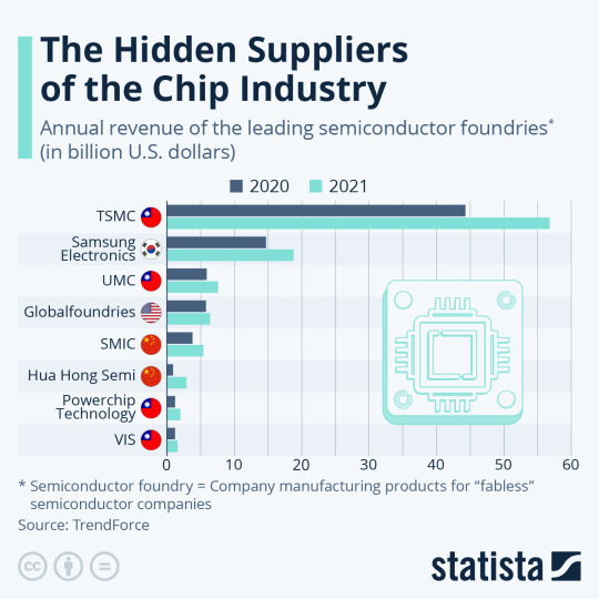
Who are the Top Chip Manufacturers in the World?
Who are the Top Chip Manufacturers in the World?
You will find more infographics at Statista
Who are the top chip manufacturers in the world?
Nearly every form of contemporary computing gadget we currently depend on to operate our daily lives is powered by silicon chips. These range from automobiles and home appliances to a number of medical gadgets, and space vehicles in addition to cell phones and computers. A large portion of our modern…
View On WordPress
#semiconductor chips#semiconductor chips for cars#semiconductor chips manufacturers#semiconductor chips manufacturing process#semiconductor#chips big name#semiconductor chips big name#semiconductor chips company#computer chips#semiconductor chips shortage#semiconductor chips 2022
0 notes
Photo

BYTE November 1995
New CPUs (including a PowerPC said to be able to also run “x86″ code even if IBM wasn’t quite explaining how yet) featured on this issue’s cover. As for what might be run with those chips, there was also a section on operating systems. It included a sidebar on Linux, mentioning it was tricky to get running but passing along the comment of a “Linux aficionado” that “If you don’t understand how it works, and how to fix it when it’s broken, you have no business using a computer.”
22 notes
·
View notes
Text
A first-ever complete map for elastic strain engineering
New Post has been published on https://thedigitalinsider.com/a-first-ever-complete-map-for-elastic-strain-engineering/
A first-ever complete map for elastic strain engineering
Without a map, it can be just about impossible to know not just where you are, but where you’re going, and that’s especially true when it comes to materials properties.
For decades, scientists have understood that while bulk materials behave in certain ways, those rules can break down for materials at the micro- and nano-scales, and often in surprising ways. One of those surprises was the finding that, for some materials, applying even modest strains — a concept known as elastic strain engineering — on materials can dramatically improve certain properties, provided those strains stay elastic and do not relax away by plasticity, fracture, or phase transformations. Micro- and nano-scale materials are especially good at holding applied strains in the elastic form.
Precisely how to apply those elastic strains (or equivalently, residual stress) to achieve certain material properties, however, had been less clear — until recently.
Using a combination of first principles calculations and machine learning, a team of MIT researchers has developed the first-ever map of how to tune crystalline materials to produce specific thermal and electronic properties.
Led by Ju Li, the Battelle Energy Alliance Professor in Nuclear Engineering and professor of materials science and engineering, the team described a framework for understanding precisely how changing the elastic strains on a material can fine-tune properties like thermal and electrical conductivity. The work is described in an open-access paper published in PNAS.
“For the first time, by using machine learning, we’ve been able to delineate the complete six-dimensional boundary of ideal strength, which is the upper limit to elastic strain engineering, and create a map for these electronic and phononic properties,” Li says. “We can now use this approach to explore many other materials. Traditionally, people create new materials by changing the chemistry.”
“For example, with a ternary alloy, you can change the percentage of two elements, so you have two degrees of freedom,” he continues. “What we’ve shown is that diamond, with just one element, is equivalent to a six-component alloy, because you have six degrees of elastic strain freedom you can tune independently.”
Small strains, big material benefits
The paper builds on a foundation laid as far back as the 1980s, when researchers first discovered that the performance of semiconductor materials doubled when a small — just 1 percent — elastic strain was applied to the material.
While that discovery was quickly commercialized by the semiconductor industry and today is used to increase the performance of microchips in everything from laptops to cellphones, that level of strain is very small compared to what we can achieve now, says Subra Suresh, the Vannevar Bush Professor of Engineering Emeritus.
In a 2018 Science paper, Suresh, Dao, and colleagues demonstrated that 1 percent strain was just the tip of the iceberg.
As part of a 2018 study, Suresh and colleagues demonstrated for the first time that diamond nanoneedles could withstand elastic strains of as much as 9 percent and still return to their original state. Later on, several groups independently confirmed that microscale diamond can indeed elastically deform by approximately 7 percent in tension reversibly.
“Once we showed we could bend nanoscale diamonds and create strains on the order of 9 or 10 percent, the question was, what do you do with it,” Suresh says. “It turns out diamond is a very good semiconductor material … and one of our questions was, if we can mechanically strain diamond, can we reduce the band gap from 5.6 electron-volts to two or three? Or can we get it all the way down to zero, where it begins to conduct like a metal?”
To answer those questions, the team first turned to machine learning in an effort to get a more precise picture of exactly how strain altered material properties.
“Strain is a big space,” Li explains. “You can have tensile strain, you can have shear strain in multiple directions, so it’s a six-dimensional space, and the phonon band is three-dimensional, so in total there are nine tunable parameters. So, we’re using machine learning, for the first time, to create a complete map for navigating the electronic and phononic properties and identify the boundaries.”
Armed with that map, the team subsequently demonstrated how strain could be used to dramatically alter diamond’s semiconductor properties.
“Diamond is like the Mt. Everest of electronic materials,” Li says, “because it has very high thermal conductivity, very high dielectric breakdown strengths, a very big carrier mobility. What we have shown is we can controllably squish Mt. Everest down … so we show that by strain engineering you can either improve diamond’s thermal conductivity by a factor of two, or make it much worse by a factor of 20.”
New map, new applications
Going forward, the findings could be used to explore a host of exotic material properties, Li says, from dramatically reduced thermal conductivity to superconductivity.
“Experimentally, these properties are already accessible with nanoneedles and even microbridges,” he says. “And we have seen exotic properties, like reducing diamond’s (thermal conductivity) to only a few hundred watts per meter-Kelvin. Recently, people have shown that you can produce room-temperature superconductors with hydrides if you squeeze them to a few hundred gigapascals, so we have found all kinds of exotic behavior once we have the map.”
The results could also influence the design of next-generation computer chips capable of running much faster and cooler than today’s processors, as well as quantum sensors and communication devices. As the semiconductor manufacturing industry moves to denser and denser architectures, Suresh says the ability to tune a material’s thermal conductivity will be particularly important for heat dissipation.
While the paper could inform the design of future generations of microchips, Zhe Shi, a postdoc in Li’s lab and first author of the paper, says more work will be needed before those chips find their way into the average laptop or cellphone.
“We know that 1 percent strain can give you an order of magnitude increase in the clock speed of your CPU,” Shi says. “There are a lot of manufacturing and device problems that need to be solved in order for this to become realistic, but I think it’s definitely a great start. It’s an exciting beginning to what could lead to significant strides in technology.”
This work was supported with funding from the Defense Threat Reduction Agency, an NSF Graduate Research Fellowship, the Nanyang Technological University School of Biological Sciences, the National Science Foundation (NSF), the MIT Vannevar Bush Professorship, and a Nanyang Technological University Distinguished University Professorship.
#1980s#applications#approach#Behavior#cellphones#change#chemistry#chips#communication#computer#computer chips#Computer modeling#cpu#crystalline#crystalline materials#defense#Design#devices#diamonds#DMSE#electron#electronic#energy#engineering#engineers#factor#form#Foundation#framework#Funding
0 notes
Text
I would do unspeakable things to her
#and all that implies.#chip originals#objectum#os/or#object sexuality#objectophilia#techum#computers
479 notes
·
View notes
Text

regret (maybe you shouldn't have fucking panini pressed your mancrush, dipshit)
#if i look at this any longer i'll lose my entire goddamn mind#is he imagining it is strahm really haunting him who's to say#oh yeah one of my friends discovered one of those dudes i'm being weird about from those saw movies is the computer chip guy from parks and#rec and i am enjoying their reaction greatly#anyway#art#illustration#my art#coffinshipping#peter strahm#mark hoffman#mark hoffman saw#peter strahm saw#is there an actual shipname for them. who's to say#saw#saw movies#hoffstrahm#saw fanart#i am consistently dogshit at tagging raise your hand if you're surprised#i'm gonna regret hitting post on this later. oh well not a now problem i will black this out of my memory#take your scraps my children#gore cw#blood cw
382 notes
·
View notes
Text
Prompt 260
You know what could be a really funny and fun crossover? Especially with my constant dragon AUs? Danny Phantom and Wakfu.
See, Danny and Tucker have decided to reincarnate together, almost like a vacation after reaching the age of 100. But see, they let Sam choose where they were going to be hanging out for the next however long, for fun!
And see, she saw world full of plants and life and an utter asshole trying to destroy a plant-person city what the fuck- and she tosses their souls into that world right away.
Now see, they didn’t really have any request about their reincarnation except that they were able to stick together. And what better way than for them to come from the same egg! Okay so maybe they arrived a little early- thank you Clockwork- but it’ll take a while to hatch anyway.
Okay, so maybe they’ve hatched alone, but that’s also fine! Sure for literal babies probably not, but they know how to do stuff- mostly. They’ll figure it out! Besides, Tucker is a freaking dragon now, and that’s so cool! And Danny has these cool wing-horns and mini portals too! Sure it’s currently only for this world, but still!
It’ll be fun, and honestly they know how to survive a desert! Mostly!
#Prompts#Danny Phantom Crossover#Wakfu Crossover#Tucker deserves to be (eventually big) serpentine dragon with a cobra hood & several horns#Danny & Tucker know technology & will figure out how to mix it with magic#Yes there is a random pair of children in the middle of the desert#Yes it is incredibly concerning#Tucker discovered his sand control means he can create most computer chips a while ago#Danny Fenton can build so many things from borderline nothing#They’ll figure it out eventually#Until then they get to enjoy being feral siblings#Tucker is delighted in the shapeshifting ability & uses it to hide the fact he’s a dragon#They have matching cloaks/hats to hide their horns#There are definitely several people concerned about the pair of desert children-toddlers they see sometimes
75 notes
·
View notes
Photo

(source)
245 notes
·
View notes
Photo

BYTE November 1996
Chips optimized to run the latest talked-up, over-the-Internet programming language featured on this issue’s cover, although inside there were comments the existing architectures were continuing to advance (as were the operating systems that ran on them), and might someday be perfectly fine running major Java applications as well.
7 notes
·
View notes
Text
‘Ruler for Light’ Could Enable Detailed Measurement in Personal Devices - Technology Org
New Post has been published on https://thedigitalinsider.com/ruler-for-light-could-enable-detailed-measurement-in-personal-devices-technology-org/
‘Ruler for Light’ Could Enable Detailed Measurement in Personal Devices - Technology Org
Frequency combs have revolutionized precision measurement, but the bulky, power-hungry devices are limited to lab settings. A new efficient laser “microcomb” developed by Stanford researchers could bring that revolution to the handheld electronics realm.
A microscope image showing a thin-film lithium niobate chip that contains eight of the new “FM-OPO” devices. One device has a footprint around 1×10 mm2 (highlighted here with a dashed rectangle). Image credit: Kevin Multani and Hubert Stokowski / Stanford University
Stanford researchers have unveiled a new type of frequency comb, a high-precision measurement device, that is innovatively small, ultra-energy efficient, and exceptionally accurate. With continued development, this breakthrough “microcomb” – which is detailed in a study published in Nature – could be the basis for mass-market adoption of the devices in everyday electronics.
Frequency combs are specialized lasers that generate evenly spaced-out lines of light akin to the teeth of a comb or, more aptly, the tick marks on a ruler. In the roughly quarter-century of their development, these “rulers for light” have revolutionized many kinds of high-precision measurement, from timekeeping to molecular detection via spectroscopy. Yet because frequency combs require bulky, costly, and power-hungry equipment, their deployment has been largely limited to laboratory settings.
The researchers discovered a workaround for these issues by integrating two different approaches for miniaturizing frequency combs into one straightforward, easily producible, microchip-style platform. Among the many applications the researchers envision for their versatile technology are powerful handheld medical diagnostic devices and widespread greenhouse gas monitoring sensors.
“The structure for our frequency comb brings the best elements of emerging microcomb technology together into one device,” said Hubert Stokowski, a postdoctoral scholar in the lab of Amir Safavi-Naeini, and lead author of the study. “We can potentially scale our new frequency microcomb for compact, low-power, and inexpensive devices that can be deployed almost anywhere.”
“We’re very excited about this new microcomb technology that we’ve demonstrated for novel types of precision sensors that are both small and efficient enough to be in someone’s phone someday,” said Safavi-Naeini, associate professor in the Department of Applied Physics at Stanford’s School of Humanities and Sciences and senior author of the study.
Wrangling light
This new device is called an Integrated Frequency-Modulated Optical Parametric Oscillator, or FM-OPO.
The tool’s complex name indicates that it combines two strategies for creating the range of distinct frequencies, or colors of light, that constitute a frequency comb. One strategy, called optical parametric oscillation, involves bouncing beams of laser light within a crystal medium, wherein the generated light organizes itself into pulses of coherent, stable waves. The second strategy centers on sending laser light into a cavity and then modulating the phase of the light – achieved by applying radio-frequency signals to the device – to ultimately produce frequency repetitions that similarly act as light pulses.
These two strategies for microcombs have not been used widely because both come with drawbacks. These issues include energy inefficiency, limited ability to adjust optical parameters, and suboptimal comb “optical bandwidth” where the comb-like lines fade as the distance from the center of the comb increases.
The researchers approached the challenge anew through their work on highly promising optical circuit platform based on a material called thin film lithium niobate. The material has advantageous properties compared to silicon, the industry standard material. Two of these helpful properties are “nonlinearity” (it allows light beams of different colors to interact with each other to generate new colors or wavelengths) and a broad range of light wavelengths can pass through it.
The researchers fashioned the components at the heart of the new frequency comb using integrated lithium niobate photonics. These light-manipulating technologies build upon advances in the related, more established field of silicon photonics, which involves fabricating optical and electronic integrated circuits on silicon microchips. In this way, lithium niobate and silicon photonics have both expanded upon the semiconductors in conventional computer chips, the roots of which reach back to the 1950s.
“Lithium niobate has certain properties that silicon doesn’t, and we couldn’t have made our microcomb device without it,” said Safavi-Naeini.
Surprisingly excellent performance
Next, the researchers brought together elements of both optical parametric amplification and phase modulation strategies. The team expected certain performance characteristics from the new frequency comb system on lithium niobate chips – but what they saw proved far better than they anticipated.
Overall, the comb produced a continuous output rather than light pulses, which enabled the researchers to reduce the required input power by approximately an order of magnitude. The device also yielded a conveniently “flat” comb, meaning the comb lines farther in wavelength from the center of the spectrum did not fade in intensity, thus offering greater accuracy and broader utility in measurement applications.
“We were really surprised by this comb,” said Safavi-Naeini. “Although we had some intuition that we would get comb-like behaviors, we weren’t really trying to make exactly this type of comb, and it took us a few months to develop the simulations and theory that explained its main properties.”
For further insight into their overperforming device, the researchers turned to Martin Fejer, the J. G. Jackson and C. J. Wood Professor of Physics and a professor of applied physics at Stanford. Along with other peers at Stanford, Fejer has helped advance modern thin film lithium niobate photonics technologies and the understanding of the material’s crystal properties.
Fejer, who is also a study co-author, made the key connection between the physical principles underlying the microcomb and ideas discussed in scientific literature from the 1970s, particularly concepts pioneered by Stephen Harris, emeritus professor of applied physics and electrical engineering at Stanford.
The new microcombs, with further honing, should be readily manufacturable at conventional microchip foundries with many practical applications such as sensing, spectroscopy, medical diagnostics, fiber-optic communications, and wearable health-monitoring devices.
“Our microcomb chip could be put into anything, with the size of the overall device depending on the size of the battery,” said Stokowski. “The technology we’ve demonstrated could go inside a low-powered personal device, the size of a phone or even smaller, and serve all kinds of useful purposes.”
To read all stories about Stanford science, subscribe to the biweekly Stanford Science Digest.
Source: Stanford University
You can offer your link to a page which is relevant to the topic of this post.
#applications#battery#challenge#chips#colors#communications#computer#computer chips#continuous#crystal#deployment#detection#development#devices#Diagnostic devices#diagnostics#electronic#Electronics#energy#engineering#equipment#Explained#fiber#Fiber-Optic#FM#frequency combs#Fundamental physics news#gas#greenhouse#greenhouse gas
0 notes
Last Seen Blogs

psycohousecat
Psycohousecat

elizabethschuyler-hamilton
i do love nothing in the world so well as you

heliosoftboxfe
Helio - SoftBox Fotos

blackbutt77
Untitled

pixelvice
PIXELVICE