#integrated circuits
Text
How a Computer Works - Part 3 (Miniaturization and Standardization)
For anyone just joining in, I'm writing a series of posts explaining perhaps haphazardly all there is to know about how a computer works, from the most basic fundamental circuitry components to whatever level of higher functionality I eventually get to. As explained in the first post on this subject, I am doing this just in pure text, so that if you are inclined you can straight up print these posts out or narrate them onto some audio tape or whatever and have full access to them should every computer in the world suddenly collapse into a pile of dust or something. Part 1 mainly covered the basic mechanical principles of circuitry and how to physically construct a logic gate. Part 2 covered logic gates in detail and how to use them to create a basic working architecture for a general purpose computer. Today we're going to be talking more about what you're looking at when you crack a machine open so you can make sense of all the important fiddly bits and have maybe a starting point on how to troubleshoot things with a multimeter or something.
Before getting into it though, I do have to shake my little donation can again and remind you that I do not know how I am going to get through the winter without becoming homeless, so if this is valuable to you, I'd appreciate some help.
Boards of Bread and Printed Circuits
With the things I've explained so far, you could totally build a computer right now, but it'd be a bit messy. You can totally buy resistors, transistors, capacitors, and diodes by the bagful for basically nothing, and cheap rolls of insulated wire, but there's all these long exposed pins to cut short and soldering things in mid-air is a messy nightmare and you'd just have this big tangle of wires in a bag or something that would almost certainly short out on you. So let's look into ways to organize stuff a little.
If you start playing around with electronics on your own, one of the first things you want to hook yourself up with besides raw components and wires is a breadboard or 12. And if you're watching people explain these things with visual aids, you'll also see a lot of them, so it's good to know exactly what they are and how they work. Your standard breadboard is a brick of plastic with a bunch of little holes in it. Incidentally, the name comes from how the first ones were literally just named after the wooden cutting boards for slicing bread people recycled to make them. Inside these holes there's some pinching bits of conductive metal which connect to each other in a particular way (pretty sure you can just see the strips that connect one if you pry the bottom off), so you can just jam a thing wire or prong into a hole, have it held in place, and make a connection to every other hole its connected to on the other side.
There is a ton of standardization to all of this. The holes should always be 0.1 inches apart () and split into two big grids. Everyone I've ever seen has 63 rows, each with 5 holes labeled A-E, a shallow channel through the middle of the board, and then another 5, F-J, and we generally have numbers printed every 5 rows. Down underneath, for any given row, the set of 5 pins on each side of the channel are connected. So, holes 1A, 1B, 1C, 1D, and 1E are all connected to each other, and nothing else. Holes 1F, 1G, 1H, 1I, and 1J are also connected to each other. There's no connection though between 1E and 1F, or 1A and 2A.
Most breadboards will also have a couple of "power rails" along the sides. These are just going to be labeled with a long red line and +, and a long blue or black line and -, and have holes in 2x5 blocks staggered out. With these, all 25 or 50 or whatever holes near the red + line connect with each other, and all the ones near the black line connect with each other. The gaps every 5 holes don't serve any purpose beyond looking different enough from the big grid so you hopefully don't mix it up and forget that these ones all connect down the length, and not in in little clumps across the width like everything else. The idea, for the sake of convention, is you plug a wire connected directly to the positive side of your battery or DC adapter or whatever into any red line hole, the negative side to any blue/black hole, and then tada, you can make a circuit just by plugging a wire in from red to a normal grid line, whatever bits you want span from that grid line to another, and eventually you connect the far end back anywhere on the black/blue line.
With a nice circuit board, there's also little snap-together pegs along the sides, and the power rails are just snapped on with those. So you can just kinda cut through the backing with a knife or some scissors, snap those off, connect multiple boards together without redundant power rails in the middle, and then just have these nice spare long lines of linked sockets. In the computer I'm building on these, I'm just using spare power rails for the bus. Oh and the big grooved channel down the middle also has a purpose. Bigger electronic components, like our good good friend the integrated circuit, are generally designed to be exactly wide enough (or more, but by a multiple of 0.1 inches) to straddle that groove as you plug their legs into the wires on either side, so they nicely fit into a breadboard, and there's a handy gap to slide something under and pry them off later on.
Typically though, you don't see breadboards inside a computer, or anything else. They're super handy for tinkering around and designing stuff, but for final builds, you want something more permanent. Usually, that's a printed circuit board, or PCB. This is pretty much what everyone's going to picture when they think about the guts of a computer. A big hard (usually) green board with a bunch of intricate lines, or "traces" running all over made of (usually) copper. And maybe with some metal ringed holes punched all the way through (they call those vias). These tend to look really complicated and maybe even a little magical, but they're honestly they're just pre-placed wires with a sense of style.
Most of the material of the board is insulated. The copper traces conduct real well, and manufacturers have done the math on just how close together they can be run without connecting to each other in places you don't want. The holes that go all the way through are for either plugging other bits in that tend to come with long legs you maybe want to keep intact, or just ways to run a trace through to the other side, where we often have traces on the back too to maximize our space. Most of what makes them look all cool and magical is how the traces run as close packed as possible to conserve space, and tend to only turn at 45 degree angles, which is just an artifact of how the machinery used to etch them out sued to be iffy about anything else.
So tada, you have all your wires pre-stuck to a nice sturdy board, and maybe even have labels printed right on there for where you solder all the various components to finish the thing. Oh and when you hear people talk about like, motherboards and daughterboards? The big main board you have for everything is a motherboard. Sometimes you need more than that, so you make smaller ones, and connect them up ether with some soldering or cartridge style with end-pins sliding snugly into sockets, and those we call daughterboards.
Integrated Circuits, or as they're also known, "chips"
The last thing you're likely to find if you crack open a computer, or just about any other electronic device that isn't super old or super super simple, are integrated circuits. Generally these are think black plastic bars that look like you'd maybe try to awkardly use them to spread cheese or peanutbutter on crackers in a prepacked snack or something, with rows of tiny little legs that running along either side. Kinda makes them look like little toy bugs or something. Sometimes they're square with pins along every edge, because sometimes you need a lot of pins. These are integrated circuits, or microchips, or just chips, and wow are they handy.
Sometime back in the 60s when people were really getting their heads around just how ridiculously small they could make electronic components and still have them work, we started to quite rapidly move towards a point where the big concern was no longer "can we shrink all this stuff down to a manageable size" and more "we are shrinking everything down to such an absurdly tiny size that we need to pack it all up in some kind of basically indestructible package, while still being able to interact with it."
So, yeah, we worked out a really solid standard there. I kinda wish I could find more on how it was set or what sort of plastic was used, but you take your absurdly shrunken down complex circuit for doing whatever. You run the teensiest tiniest wires you can out from it that thicken up at the ends into standard toothy prongs you can sink into a breadboard or a PCB with that standardized pin spacing, and you coat it all in this black plastic so firmly enveloping it that nothing can move around inside or get broken, hopefully.
And honestly, in my opinion, this is all TOO standardized. The only real visible difference between any two given integrated circuits is how many legs they have, and even those tend to come to some pretty standard numbers. They're always the same size shape and color, they all have the same convention of having a little indented notch on one side so you know which end is which, and they all seem to use just the worst ink in the world to print a block of numbers on the back with their manufacturer, date of assembly, a catalog number, and some other random stuff.
For real if there's any real comprehensive standard for what's printing on these, I can't for the life of me find it. All I know is, SOMEWHERE, you've got a 2 or 3 letter code for every manufacturer, a number for the chip, and a 4 digit date code with the last 2 digits of the year, and which week of that year it was. These three things can be in any order, other things can also be on there, probably with zero spacing, and usually printed in ink that wipes away like immediately or at least is only readable under really direct light, it sucks.
Once you know what a chip is though and look up the datasheet for it, you should have all sorts of handy info on what's inside, and just need to know what every leg is for. For that, you find which end has a notch in it, that's the left side, sometimes there's also a little dot in the lower left corner, and hopefully the label is printed in alignment with that. From there, the bottom left leg is pin 1, and then you count counterclockwise around the whole chip. You're basically always going to have positive and negative power pins, past that anything goes. You can cram a whole computer into a single chip, yo can have someone just put like 4 NAND gates on a chip for convenience, whatever.
OK, but how do they make them so small?
OK, so, mostly a circuit we're going to want to shrink down and put on a chip is just gonna be a big pile of logic gates, we can make our logic gates just using transistors, and we can make transistors just by chemically treating some silicon. So we just need SUPER flat sheets of treated silicon, along with some little strands of capacitive/resistive/insulating material here and there, and a few vertically oriented bits of conductive metal to pass signals up and down as we layer these together. Then we just need to etch them out, real real small and tight.
And we can do that etching at like, basically infinite resolution it turns out. It just so happens we have access to special acids that eat through the materials we need them to eat through, but that only work when they're being directly hit with fairly intense UV light. And a thing about light is when you have say, a big cut out pattern that you hold between a light and a surface, it casts a shadow on it... and the scaling of that shadow depends entirely on the distances between the light, the pattern, and the surface. So if you're super careful calibrating everything, you can etch a pattern into something at a scale where the main limiting factors become stuff like how many molecules thick things have to be to hold their shape. Seriously, they use electron microscopes to inspect builds because that's the level of tininess we have achieved.
So yeah, you etch your layers of various materials out with shadow masks and UV acid, you stack them up, you somehow align microscopic pins to hold them together and then you coat the whole mess in plastic forever. Tada. Anything you want in a little chip.
ROMs, maybe with various letters in front
So there's a bunch of standard generally useful things people put into ICs, but also with a computer you generally want some real bespoke stored values with a lookup table where you'll keep, say, a program to be run by feeding whatever's inside out to the bus line by line. For that we use a chip we call Read Only Memory, or ROM. Nothing super special there, just... hard wire in the values you need when you manufacture it. Manufacturing these chips though is kind of a lot, with the exacting calibrations and the acid and the clean rooms and all. Can't we have some sort of Programmable ROM? Well sure, just like build it so that all the values are 1, and build a special little thing that feeds more voltage through than it can handle and physically destroy the fuse for everything you don't want to be a 1.
OK that's still kind of a serious commitment. What if I want to reuse this later? Oh, so you want some sort of Erasable PROM? OK someone came up with a funky setting where you overload and blow out the fuses but then if you expose the guts of the chip to direct UV light through this little window, everything should reform back to 1. Just like, throw a sticker on there when you don't want to erase it. Well great, but can we maybe not have me desolder it and take it out to put under a lamp? Oh la de da! You need Electronically Erasable PROMs? EEPROMs? I guess we can make THAT work, somehow. They're still gonna be slow to write to though, can't have anything. I mean, not unless we invented like, flash memory. Which somehow does all this at speeds where you can use it for long term storage without it being a pain. So that's just kinda the thing we have now. Sorry I don't quite get the principles behind it enough to summarize. Something about floating components and needing less voltage or whatever. Apparently you sacrifice some read speed next to older options but hey, usable rewritable long term storage you just plug in, no jumping through extra hoops.
So OK. I think that's everything I can explain without biting the bullet and explaining ALUs and such. Well, there's keyboards (they're just buttons connecting input lines), monitors (these days, LEDs wired up in big grids), and mice (there's spokes in wheels that click X times or cameras checking the offset values of dust on your desk or whatnot).
Maybe throw me some money before we move on ?
CONTINUED IN PART 4
#computers#computer science#pcb#printed circuit board#integrated circuits#microchip#breadboards#education#electronics
54 notes
·
View notes
Text
Some kind of arachnid…
Can I get help with an id?
youtube
8 notes
·
View notes
Text
IGCT: Powering the Future of Electronics
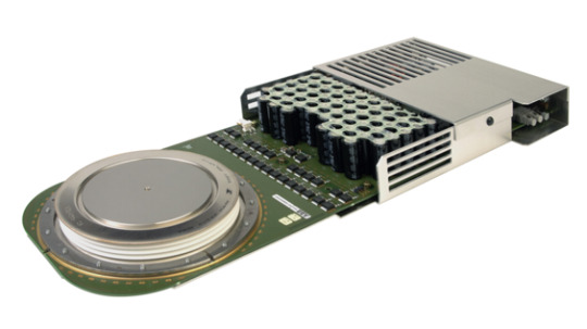
IGCT (Integrated Gate Commutated Thyristors) is a powerful and versatile power semiconductor device widely utilized in the electronic components industry. With its exceptional performance, fast switching speed, and high current-carrying capability, IGCT has found extensive applications in power transmission, industrial drives, and power electronics.
Knowing more: smbom.com
2 notes
·
View notes
Text
Exploring the World of Integrated Circuits Base: 40 Pin Wide IC Base
Integrated circuits (ICs) are the building blocks of modern electronics, and they come in a range of shapes and sizes. An IC base is a component that holds an IC in place and allows it to be readily replaced or removed. In this article, we will look at the 40 Pin Wide IC Base, which is a specialty IC base built to hold ICs with 40 pins.
The 40 Pin Wide IC Base is a high-quality component utilised in a variety of electrical applications. It is intended to support ICs with 40 pins and is larger in size than other IC bases to accommodate the greater number of pins. Its IC base is normally constructed of high-quality materials such as plastic or ceramic, ensuring its robustness and lifespan.
The 40-Pin Wide IC Base's pins are organized in two rows, making it simple to install and remove the IC. The IC is positioned on top of the base, with its pins aligned with the appropriate pins on the base. Once the IC is in position, the base secures it, and the IC's pins establish contact with the pins on the base.
The 40 Pin Wide IC Base is perfect for applications that require the IC to be securely held in place and have adequate area to support the larger size. This integrated circuit base is widely utilized in electronic applications such as microcontrollers, memory modules, and digital signal processors. One advantage of adopting the 40 Pin Wide IC Base is that the IC can be easily replaced. If the IC is broken or has to be improved, it is simple to remove it from the base and replace it with a new IC. This facilitates the repair or upgrade of electronic devices, which is particularly important for industrial or commercial applications.
3 notes
·
View notes
Text
How to Identify and Replace a Faulty IC?
If you're experiencing issues with your device and suspect a faulty Integrated Circuits, here's a guide to help you identify and replace it.
Visual Inspection: Start by visually inspecting the IC for any signs of damage, such as cracks, discoloration, or burn marks. These are clear indicators of a faulty IC.
Testing with a Multimeter: Use a multimeter to check the continuity and resistance of the IC's pins. A significant deviation from the expected values could indicate a faulty IC.
Using an IC Tester: If available, use an IC tester to perform a comprehensive test on the IC. The tester will check the functionality of the IC and identify any faults.
Testing in a Circuit: If possible, remove the IC from the circuit and test it separately using appropriate test equipment. This will help isolate the IC as the source of the problem.
Replacing a Faulty IC
Identify the IC: Before replacing the IC, ensure you have the correct replacement part. Note down the part number and manufacturer of the faulty IC.
Prepare the Replacement: Carefully remove the faulty IC from the circuit using a disordering tool. Be mindful of the surrounding components to avoid damage.
Install the Replacement: Insert the new IC into the circuit, ensuring the orientation is correct. Use a soldering iron to solder the pins of the new IC to the circuit board.
Test the Replacement: Once the new IC is installed, power on the device and test its functionality. If the replacement was successful, the device should now operate correctly.
0 notes
Text
PCB Design and Assembly with Chengsuchuang.com
Discover top-quality PCB assembly solutions at Chengsuchuang.com. From prototype to mass production, our expert team ensures precision, reliability, and timely delivery. Explore our comprehensive services for your electronic manufacturing needs.
0 notes
Text
Factorio is an exercise in logistical planning. Or in my case, a circuit designer. I've spent the last two hours trying to get a three-way split distribution node pre-emptively designed for 10 raw ingredients inside a single 32x32 tile grid chunk. Unfortunately, I can almost do it but those belts are going to have to cart along two different item types. And yes, it is outputting the same order as the input bus.
....Sonofa, maybe if I didn't have boxes acting as buffers, or have the outputs in the same node.... >,,< God...damn...it. That would work...
0 notes
Text
Integrated Circuits Hub: Find Your Perfect Component Here
Discover a vast array of Integrated Circuits at express-technology.com. Explore an extensive selection catering to diverse applications and specifications. Find cutting-edge IC solutions from renowned brands, empowering technological innovation across industries. Streamline your search for high-quality integrated circuits tailored to your specific needs.
0 notes
Text
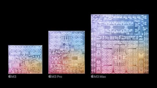
So, these are Apple's brand new M3 CPU chips. I don’t know the scale, but I imagine the one on the right is about an inch across.
Per AnandTech, these contain 25 billion, 37 billion and 92 billion transistors each. The features transistors and wires) on the chips are 3 nanometers (3 billionths of a meter) across, which is a new record in resolution set by manufacturer TSMC.
I like to think I’m immured to future shock since I grew up with this stuff (my dad worked for chip pioneer Fairchild in the 70s and would bring home ICs and wafers for kid-me) but HOLY FUCK.
To get technical: a transistor is something like an Oreo. Two layers of one material separated by a filling of a different material. Except both are impure silicon. Applying a voltage to the middle layer switches current between the top and bottom layers on or off. These used to be packaged as little metal cans the size of a pencil eraser with three wires coming out (still are, if they’re being used in guitar pedals…)
So the M3 Max chip contains NINETY-TWO FUCKING BILLION of those, plus miles of wiring between them. That’s 11+ transistors, a handful of little cans, for every human on Earth.
And these can be churned out on assembly lines by the millions. You can’t buy an individual M3 but they’re probably worth a few hundred bucks; but there are plenty of lower end CPUs — “systems on a chip” — with maybe only one billion transistors, that sell for 10¢ on electronics market sites like AliExpress. For five or ten dollars you can buy a little stick of gum like a Raspberry Pi Zero that you can plug a keyboard and screen into and use as a PC.
And how small are these 3 nanometer transistors? A nanometer is a billionth of a meter, or roughly 20 millionths of an inch.
A human hair is about 75,000 nm across
A red blood cell is 6,000 nm across
A silicon atom is about 2nm across (in a very blurry way)
Humans today are manufacturing machines, at high volume, whose components are LITERALLY THE SIZE OF A FEW ATOMS. That is absolutely insane.
The early chips my dad brought home from work had maybe a few hundred transistors. I put a chip under my crappy kid microscope and could see them individually. That was 50 years ago. Now the transistors are literally too small to be seen, because they’re a lot smaller than the wavelength of visible light.
OK, I’m an old guy rambling. But I think we — myself included — spend too much time idly staring at the devices in our hands and on our desks, and not enough time gazing at them in abject awe.
We did this. Humans did this. We can do unbelievable, amazing shit when we try and try and keep working to make things better.
We have to somehow figure out how to make ourselves, our hearts and ethics, better. We can make a billion angels dance on the head of a pin; why are we still killing each other, hating each other, letting each other starve?
0 notes
Text
A "bit" of computing history from 40 years ago.
ARM CPUs are still popular today, particularly in smartphones, so the next installment of this history should be even more interesting.
#information technology#computing history#ars technica#computer chips#integrated circuits#computer architecture#computer engineering#1980s
0 notes
Text
What Are IOC Elements?

Integrated Optical Circuit (IOC) elements represent a crucial advancement in the realm of electronic components, seamlessly integrating optical and electronic functionalities onto a single chip. The core innovation lies in the amalgamation of optical and electronic devices, facilitating the processing and transmission of optical signals. This breakthrough not only propels the evolution of optoelectronic technology but also injects fresh vitality into the electronic components industry.
Get more details: What Are IOC Elements?
#electronics#integrated circuits#semiconductor#components#electronic#module#electronic devices#chips#manufacturing#package
0 notes
Text

Old IC made in czechoslovakia (by tesla)
Ram module MHB 4116
1 note
·
View note
Text
Battery management circuit, integrated circuits, Voltage Converter
VIPer01 Series 30 V 60 kHz Energy Saving Off-Line High Voltage Converter-SSOP-10
0 notes
Text
Cmos logic ic, integrated circuits, 4000 series CMOS Logic ICs, nand gate ic
4000B Series 3 to 15 V Quad 2-Input NAND Schmitt Trigger Surface Mount - SOIC-14
0 notes
Text
Understanding the 74LS90 Pinout: A Comprehensive Guide
If you're diving into digital electronics, you'll soon realize how integral certain ICs are. The 74LS90, a 4-bit decade counter, is one of them. But to effectively use it in your projects, understanding its pinout is essential. Let's jump in and dissect this little marvel!
What is the 74LS90?
Before diving into the pinout details, a quick recap. The 74LS90 is a 4-bit decade counter, which means it can count from 0 to 9. When used in specific configurations, it can also be employed as a binary counter (0-15). It belongs to the 74LS (Low-power Schottky) TTL (Transistor-Transistor Logic) family, known for its balance of speed and power consumption.
Pin Configuration
The 74LS90 IC has a standard 14-pin configuration. Here's a detailed breakdown of each pin:
Pin 1 (Reset A): When this pin goes HIGH, it resets the count to zero. It's often connected to ground (LOW) if you don’t want the counter to reset before reaching 9.
Pin 2 (Reset B): This pin works in conjunction with Reset A. Both pins must be set HIGH simultaneously to reset the counter.
Pin 3 (Clock B): This pin is used to provide clock pulses for counting. The counter advances on the rising edge of the clock.
Pin 4 (Clock A): Clock A receives clock pulses and controls the first flip-flop. Typically, this pin receives output from Clock B.
Pin 5 (Output D): Represents the 2^3 or 8's place in the 4-bit binary output.
Pin 6 (Output C): Represents the 2^2 or 4's place in the 4-bit binary output.
Pin 7 (GND): This is the ground pin and is connected to the negative terminal of the supply voltage.
Pin 8 (Output B): Represents the 2^1 or 2's place in the 4-bit binary output.
Pin 9 (Output A): Represents the 2^0 or 1's place in the 4-bit binary output.
Pin 10 (Set B): This is the preset input of the second flip-flop. When set HIGH, the flip-flop goes to a SET state.
Pin 11 (Set A): The preset input for the first flip-flop. When HIGH, this flip-flop goes to the SET state.
Pin 12 (Output E): Represents the overflow or carry-out. This pin goes HIGH when the counter overflows from 9 back to 0.
Pin 13 (Output F): An auxiliary output that can be used for cascading multiple 74LS90s.
Pin 14 (Vcc): This is the power supply pin and should be connected to the positive terminal of the supply voltage (typically 5V for TTL logic).
Using the 74LS90
Now that you understand each pin's function, using the IC becomes a lot easier. Remember:
Always connect the GND (Pin 7) and Vcc (Pin 14) correctly. Incorrect power connections can damage the IC.
When using it as a decade counter, monitor the outputs A, B, C, and D. They provide the binary equivalent of the decimal number being counted.
For applications requiring counts above 9, consider cascading multiple 74LS90s using the Output E and Output F pins.
Conclusion
Understanding the pinout of an IC like the 74LS90 is fundamental to using it effectively in any project. With the knowledge you've acquired from this guide, you're well-equipped to design circuits, troubleshoot issues, and explore more advanced configurations with the 74LS90.
0 notes
Text
What is transistor, integrated circuits, Metal Oxide Semiconductor, Power MOSFET
P-Channel 20 V 44 mOhm 8.3 W Surface Mount Power MOSFET - SOT-223
0 notes
Last Seen Blogs

sa-you
Sayou.

classytriumphlady
Untitled

axelotyls
lesbian disaster

objectifbucketlist
Objectif Bucket List

airymaria
if you know me IRL, no you dont