#printed circuit board
Text
How a Computer Works - Part 3 (Miniaturization and Standardization)
For anyone just joining in, I'm writing a series of posts explaining perhaps haphazardly all there is to know about how a computer works, from the most basic fundamental circuitry components to whatever level of higher functionality I eventually get to. As explained in the first post on this subject, I am doing this just in pure text, so that if you are inclined you can straight up print these posts out or narrate them onto some audio tape or whatever and have full access to them should every computer in the world suddenly collapse into a pile of dust or something. Part 1 mainly covered the basic mechanical principles of circuitry and how to physically construct a logic gate. Part 2 covered logic gates in detail and how to use them to create a basic working architecture for a general purpose computer. Today we're going to be talking more about what you're looking at when you crack a machine open so you can make sense of all the important fiddly bits and have maybe a starting point on how to troubleshoot things with a multimeter or something.
Before getting into it though, I do have to shake my little donation can again and remind you that I do not know how I am going to get through the winter without becoming homeless, so if this is valuable to you, I'd appreciate some help.
Boards of Bread and Printed Circuits
With the things I've explained so far, you could totally build a computer right now, but it'd be a bit messy. You can totally buy resistors, transistors, capacitors, and diodes by the bagful for basically nothing, and cheap rolls of insulated wire, but there's all these long exposed pins to cut short and soldering things in mid-air is a messy nightmare and you'd just have this big tangle of wires in a bag or something that would almost certainly short out on you. So let's look into ways to organize stuff a little.
If you start playing around with electronics on your own, one of the first things you want to hook yourself up with besides raw components and wires is a breadboard or 12. And if you're watching people explain these things with visual aids, you'll also see a lot of them, so it's good to know exactly what they are and how they work. Your standard breadboard is a brick of plastic with a bunch of little holes in it. Incidentally, the name comes from how the first ones were literally just named after the wooden cutting boards for slicing bread people recycled to make them. Inside these holes there's some pinching bits of conductive metal which connect to each other in a particular way (pretty sure you can just see the strips that connect one if you pry the bottom off), so you can just jam a thing wire or prong into a hole, have it held in place, and make a connection to every other hole its connected to on the other side.
There is a ton of standardization to all of this. The holes should always be 0.1 inches apart () and split into two big grids. Everyone I've ever seen has 63 rows, each with 5 holes labeled A-E, a shallow channel through the middle of the board, and then another 5, F-J, and we generally have numbers printed every 5 rows. Down underneath, for any given row, the set of 5 pins on each side of the channel are connected. So, holes 1A, 1B, 1C, 1D, and 1E are all connected to each other, and nothing else. Holes 1F, 1G, 1H, 1I, and 1J are also connected to each other. There's no connection though between 1E and 1F, or 1A and 2A.
Most breadboards will also have a couple of "power rails" along the sides. These are just going to be labeled with a long red line and +, and a long blue or black line and -, and have holes in 2x5 blocks staggered out. With these, all 25 or 50 or whatever holes near the red + line connect with each other, and all the ones near the black line connect with each other. The gaps every 5 holes don't serve any purpose beyond looking different enough from the big grid so you hopefully don't mix it up and forget that these ones all connect down the length, and not in in little clumps across the width like everything else. The idea, for the sake of convention, is you plug a wire connected directly to the positive side of your battery or DC adapter or whatever into any red line hole, the negative side to any blue/black hole, and then tada, you can make a circuit just by plugging a wire in from red to a normal grid line, whatever bits you want span from that grid line to another, and eventually you connect the far end back anywhere on the black/blue line.
With a nice circuit board, there's also little snap-together pegs along the sides, and the power rails are just snapped on with those. So you can just kinda cut through the backing with a knife or some scissors, snap those off, connect multiple boards together without redundant power rails in the middle, and then just have these nice spare long lines of linked sockets. In the computer I'm building on these, I'm just using spare power rails for the bus. Oh and the big grooved channel down the middle also has a purpose. Bigger electronic components, like our good good friend the integrated circuit, are generally designed to be exactly wide enough (or more, but by a multiple of 0.1 inches) to straddle that groove as you plug their legs into the wires on either side, so they nicely fit into a breadboard, and there's a handy gap to slide something under and pry them off later on.
Typically though, you don't see breadboards inside a computer, or anything else. They're super handy for tinkering around and designing stuff, but for final builds, you want something more permanent. Usually, that's a printed circuit board, or PCB. This is pretty much what everyone's going to picture when they think about the guts of a computer. A big hard (usually) green board with a bunch of intricate lines, or "traces" running all over made of (usually) copper. And maybe with some metal ringed holes punched all the way through (they call those vias). These tend to look really complicated and maybe even a little magical, but they're honestly they're just pre-placed wires with a sense of style.
Most of the material of the board is insulated. The copper traces conduct real well, and manufacturers have done the math on just how close together they can be run without connecting to each other in places you don't want. The holes that go all the way through are for either plugging other bits in that tend to come with long legs you maybe want to keep intact, or just ways to run a trace through to the other side, where we often have traces on the back too to maximize our space. Most of what makes them look all cool and magical is how the traces run as close packed as possible to conserve space, and tend to only turn at 45 degree angles, which is just an artifact of how the machinery used to etch them out sued to be iffy about anything else.
So tada, you have all your wires pre-stuck to a nice sturdy board, and maybe even have labels printed right on there for where you solder all the various components to finish the thing. Oh and when you hear people talk about like, motherboards and daughterboards? The big main board you have for everything is a motherboard. Sometimes you need more than that, so you make smaller ones, and connect them up ether with some soldering or cartridge style with end-pins sliding snugly into sockets, and those we call daughterboards.
Integrated Circuits, or as they're also known, "chips"
The last thing you're likely to find if you crack open a computer, or just about any other electronic device that isn't super old or super super simple, are integrated circuits. Generally these are think black plastic bars that look like you'd maybe try to awkardly use them to spread cheese or peanutbutter on crackers in a prepacked snack or something, with rows of tiny little legs that running along either side. Kinda makes them look like little toy bugs or something. Sometimes they're square with pins along every edge, because sometimes you need a lot of pins. These are integrated circuits, or microchips, or just chips, and wow are they handy.
Sometime back in the 60s when people were really getting their heads around just how ridiculously small they could make electronic components and still have them work, we started to quite rapidly move towards a point where the big concern was no longer "can we shrink all this stuff down to a manageable size" and more "we are shrinking everything down to such an absurdly tiny size that we need to pack it all up in some kind of basically indestructible package, while still being able to interact with it."
So, yeah, we worked out a really solid standard there. I kinda wish I could find more on how it was set or what sort of plastic was used, but you take your absurdly shrunken down complex circuit for doing whatever. You run the teensiest tiniest wires you can out from it that thicken up at the ends into standard toothy prongs you can sink into a breadboard or a PCB with that standardized pin spacing, and you coat it all in this black plastic so firmly enveloping it that nothing can move around inside or get broken, hopefully.
And honestly, in my opinion, this is all TOO standardized. The only real visible difference between any two given integrated circuits is how many legs they have, and even those tend to come to some pretty standard numbers. They're always the same size shape and color, they all have the same convention of having a little indented notch on one side so you know which end is which, and they all seem to use just the worst ink in the world to print a block of numbers on the back with their manufacturer, date of assembly, a catalog number, and some other random stuff.
For real if there's any real comprehensive standard for what's printing on these, I can't for the life of me find it. All I know is, SOMEWHERE, you've got a 2 or 3 letter code for every manufacturer, a number for the chip, and a 4 digit date code with the last 2 digits of the year, and which week of that year it was. These three things can be in any order, other things can also be on there, probably with zero spacing, and usually printed in ink that wipes away like immediately or at least is only readable under really direct light, it sucks.
Once you know what a chip is though and look up the datasheet for it, you should have all sorts of handy info on what's inside, and just need to know what every leg is for. For that, you find which end has a notch in it, that's the left side, sometimes there's also a little dot in the lower left corner, and hopefully the label is printed in alignment with that. From there, the bottom left leg is pin 1, and then you count counterclockwise around the whole chip. You're basically always going to have positive and negative power pins, past that anything goes. You can cram a whole computer into a single chip, yo can have someone just put like 4 NAND gates on a chip for convenience, whatever.
OK, but how do they make them so small?
OK, so, mostly a circuit we're going to want to shrink down and put on a chip is just gonna be a big pile of logic gates, we can make our logic gates just using transistors, and we can make transistors just by chemically treating some silicon. So we just need SUPER flat sheets of treated silicon, along with some little strands of capacitive/resistive/insulating material here and there, and a few vertically oriented bits of conductive metal to pass signals up and down as we layer these together. Then we just need to etch them out, real real small and tight.
And we can do that etching at like, basically infinite resolution it turns out. It just so happens we have access to special acids that eat through the materials we need them to eat through, but that only work when they're being directly hit with fairly intense UV light. And a thing about light is when you have say, a big cut out pattern that you hold between a light and a surface, it casts a shadow on it... and the scaling of that shadow depends entirely on the distances between the light, the pattern, and the surface. So if you're super careful calibrating everything, you can etch a pattern into something at a scale where the main limiting factors become stuff like how many molecules thick things have to be to hold their shape. Seriously, they use electron microscopes to inspect builds because that's the level of tininess we have achieved.
So yeah, you etch your layers of various materials out with shadow masks and UV acid, you stack them up, you somehow align microscopic pins to hold them together and then you coat the whole mess in plastic forever. Tada. Anything you want in a little chip.
ROMs, maybe with various letters in front
So there's a bunch of standard generally useful things people put into ICs, but also with a computer you generally want some real bespoke stored values with a lookup table where you'll keep, say, a program to be run by feeding whatever's inside out to the bus line by line. For that we use a chip we call Read Only Memory, or ROM. Nothing super special there, just... hard wire in the values you need when you manufacture it. Manufacturing these chips though is kind of a lot, with the exacting calibrations and the acid and the clean rooms and all. Can't we have some sort of Programmable ROM? Well sure, just like build it so that all the values are 1, and build a special little thing that feeds more voltage through than it can handle and physically destroy the fuse for everything you don't want to be a 1.
OK that's still kind of a serious commitment. What if I want to reuse this later? Oh, so you want some sort of Erasable PROM? OK someone came up with a funky setting where you overload and blow out the fuses but then if you expose the guts of the chip to direct UV light through this little window, everything should reform back to 1. Just like, throw a sticker on there when you don't want to erase it. Well great, but can we maybe not have me desolder it and take it out to put under a lamp? Oh la de da! You need Electronically Erasable PROMs? EEPROMs? I guess we can make THAT work, somehow. They're still gonna be slow to write to though, can't have anything. I mean, not unless we invented like, flash memory. Which somehow does all this at speeds where you can use it for long term storage without it being a pain. So that's just kinda the thing we have now. Sorry I don't quite get the principles behind it enough to summarize. Something about floating components and needing less voltage or whatever. Apparently you sacrifice some read speed next to older options but hey, usable rewritable long term storage you just plug in, no jumping through extra hoops.
So OK. I think that's everything I can explain without biting the bullet and explaining ALUs and such. Well, there's keyboards (they're just buttons connecting input lines), monitors (these days, LEDs wired up in big grids), and mice (there's spokes in wheels that click X times or cameras checking the offset values of dust on your desk or whatnot).
Maybe throw me some money before we move on ?
CONTINUED IN PART 4
#computers#computer science#pcb#printed circuit board#integrated circuits#microchip#breadboards#education#electronics
54 notes
·
View notes
Text

77 notes
·
View notes
Text

A spare PCB given to me at VCF Midwest years ago, full of (hopefully) useful switches.
41 notes
·
View notes
Text

Printed Circuit Board Stormtrooper
14 notes
·
View notes
Text
0 notes
Text
Optimizing Assembly Processes for High-Quality PCBs: Best Practices and Technologies
Printed Circuit Boards (PCBs) are the fundamental building blocks of electronic devices, and the quality of their assembly plays a crucial role in the overall performance and reliability of these devices. As technology advances and demands for smaller, more complex PCBs increase, optimizing assembly processes becomes paramount. In this article, we delve into the best practices and technologies for achieving high-quality PCB assembly.
Understanding High-Quality PCB Assembly
High-quality PCB assembly goes beyond merely soldering components onto a board. It involves a combination of precision engineering, meticulous planning, rigorous quality control, and adherence to industry standards. The goal is to produce PCBs that meet or exceed performance specifications, have minimal defects, and ensure long-term reliability in diverse operating conditions.
Best Practices for Optimizing PCB Assembly
Design for Manufacturability (DFM): Begin the optimization process during the PCB design phase by considering manufacturability aspects such as component placement, trace routing, and thermal management. DFM principles help minimize assembly challenges and ensure smooth production.
Component Quality and Selection: Use high-quality components from reputable suppliers to minimize the risk of component failures. Select components that meet the required specifications for performance, reliability, and compatibility with assembly processes.
SMT vs. Through-Hole Assembly: Evaluate the suitability of Surface Mount Technology (SMT) versus Through-Hole assembly based on design requirements, component sizes, and production volume. SMT offers advantages in miniaturization, higher component densities, and automated assembly capabilities.
Optimized Soldering Techniques: Employ advanced soldering techniques such as reflow soldering, wave soldering, or selective soldering based on the complexity of the PCB and component types. Optimize solder paste application, stencil design, and reflow profiles for consistent solder joints and minimal defects.
Automated Assembly Equipment: Invest in modern automated assembly equipment such as pick-and-place machines, solder paste printers, reflow ovens, and inspection systems. Automation improves efficiency, accuracy, and repeatability while reducing manual errors.
Quality Control and Testing: Implement robust quality control measures throughout the assembly process, including visual inspection, automated optical inspection (AOI), X-ray inspection, and functional testing. Detect defects early, identify root causes, and take corrective actions to ensure high-quality outputs.
Training and Skill Development: Train assembly technicians and engineers on the latest assembly techniques, equipment operation, and quality standards. Continuously update skills and knowledge to adapt to evolving technologies and industry best practices.
Technologies for Enhanced Assembly Processes
Automated Optical Inspection (AOI): AOI systems use high-resolution cameras and image processing algorithms to inspect PCBs for defects such as soldering defects, component placement errors, and trace discontinuities. AOI improves defect detection rates and reduces inspection time.
X-ray Inspection: X-ray inspection is valuable for inspecting hidden solder joints, checking component alignment, and identifying defects in complex PCBs with multiple layers. It ensures the integrity of critical connections and detects defects that may not be visible to the naked eye.
Selective Soldering Systems: Selective soldering machines target specific areas of the PCB for soldering, allowing precise control over soldering parameters and reducing thermal stress on sensitive components. This technology is beneficial for assemblies with mixed technologies and selective solder requirements.
Advanced Solder Paste and Fluxes: Use high-quality solder paste formulations and fluxes optimized for specific assembly processes and component types. Low-residue fluxes, no-clean fluxes, and lead-free solder options contribute to cleaner, more reliable solder joints.
Conclusion
Optimizing assembly processes for high-quality PCBs requires a holistic approach that encompasses design considerations, best practices, advanced technologies, and a commitment to continuous improvement. By integrating DFM principles, selecting quality components, leveraging automated equipment, implementing robust quality control measures, and adopting advanced inspection technologies, manufacturers can achieve superior PCB assembly outcomes. Embracing innovation and investing in skills development are key to staying competitive in the dynamic landscape of electronic manufacturing.
0 notes
Text
PCB Manufacturing

PCB manufacturing is a precision process involving designing, etching, and assembling printed circuit boards. We specialize in producing high-quality PCBs tailored to your specifications. Our advanced technology and rigorous quality control ensure reliability and performance. Trust us for efficient and cost-effective PCB manufacturing solutions to meet your electronic needs.
Visit Our Site: https://sqpcb.com/products/pcb-manufacture
#customized pcb boards#customize pcb#pcb board#pcb china#aluminium pcb board#multilayer pcb#printed circuit board#aluminum base pcb#circuit board#custom circuit boards
0 notes
Text
What is Rigid-Flex Circuit Board?
Rigid-flex PCB board, it is a circuit board that combines flexible and rigid circuit board technology in the application. Most rigid-flex boards are composed of multiple layers of flexible circuit boards, which are attached to one or more rigid boards from the outside and/or from the inside, depending on the design of the application. The flexible substrate is designed to be in a constant deflection state, and is usually formed as a deflection curve during rigid flex pcb manufacturing or assembly.
The Production Process of Rigid-Flex PCB
Rigid flex PCB production is based on below steps: the first step is to process the rigid outer cover layer. The electroplating graphic that needs to be pressed in the outer layer, and then through the CNC milling machine, punching or laser method, routing out or routing the half of depth of the flexible part which is located in rigid layer. Flex board and the rigid outer cover are boned by adhesive sheet. The adhesive sheet has been pre-opened in the flexible part.
During the lamination process, if the rigid outer layer uses routing structure, a suitable pressure filling board should be prepared for the flex part. Using a vacuum pressing machine to obtain better press quality, and meanwhile with some auxiliary coating materials, such as PE, etc., so that the pressing process can provide a uniform pressure on the entire board, and make the low -flowing sticky sheet is fully flowing and filling the gap, especially for complex structures. Before adhesion or lamination, appropriate baking should be done as needed to remove moisture.
After lamination, the rigid- flex PCB can use a through hole treatment process which is similar to a multi-layer rigid board, the different part is remove drilling dirt. The method of removing drilling dirt depends on what materials used. Like the rigid board, drilling the hole after fully baking, and then use the plasma etching process to remove the residue in the hole wall. Before the plasma is treated, bake is also needed to remove water vapor. Caval polyesterness is generally recommended to not exceed 13um. The pore -plating process of conventional rigid board can be used, but the specific process parameters of the electroplating should be determined according to the reliability test data of the pores.

The Rigid-Flex manufacturing phase is also more complex and time-consuming than rigid board fabrication. All the flexible components of the Rigid-Flex assembly have completely different handling, etching, and soldering processes than rigid FR4 boards.
Benefits of Rigid Flex PCB
·Space requirements can be minimized by applying 3D
·By removing the need for connectors and cables between the individual rigid parts the board size and overall system weight can be reduced.
·By maximizing space, there is often a lower count in parts.
·Less solder joints assure higher connection reliability.
·Handling during assembly is easier in comparison with flexible boards.
·Simplified PCB assembly processes.
·Integrated ZIF contacts provide simple modular interfaces to the system environment.
·Test conditions are simplified. A complete test prior to installation becomes possible.
·Logistical and assembly costs are significantly reduced with flex-rigid boards.
·It is possible to increase the complexity of mechanical designs, which also improves the degree of freedom for optimized housing solutions.
Rigid Flex PCB Fabrication Applications
Rigid flexible PCBs offer a wide array of applications, ranging from military weaponry and aerospace systems to cell phones and digital cameras. Increasingly, rigid flex board fabrication has been used in medical devices such as pacemakers for their space and weight reduction capabilities. The same advantages for rigid flex PCB usage can be applied to military weaponry and weapon control systems
In consumer products, rigid flex doesn’t just maximize space and weight but greatly improves reliability, eliminating many needs for solder joints and delicate, fragile wiring that are prone to connection issues. These are just some examples, but rigid flex PCBs can be used to benefit nearly all advanced electrical applications including testing equipment, tools and automobiles.
Available structures for rigid flex PCB
There are numerous, different structures available. The more common ones are defined below:
Traditional rigid flex construction (IPC-6013 type 4) Multilayer rigid and flexible circuit combination containing three or more layers with plated through holes.
Asymmetrical rigid flex construction, where the FPC is situated on the outer layer of the rigid construction. Containing three or more layers with plated through holes.
Multilayer rigid flex construction with buried / blind via (microvia) as part of the rigid construction. 2 layers of microvia are achievable. Construction may also include two rigid structures as part of a homogeneous build.
The Advantages of Rigid-Flex PCB
One of the key features of rigid-flex PCB is the thin profile and changeable shape, making it an ideal solution for ultra -thin and ultra -light packaging. Although the rigid flex PCB may be more expensive in design and manufacturing, they do have many advantages and can solve many problems in traditional hardboard technology.
1. Small Size and Flexible Shape
The rigid- flex PCB is easier to install more components in smaller space, because they can change the shape according to a specific contour. This technology will reduce the size and weight of the final product and the overall system cost. At the same time, the compact shape of rigid flex PCB makes it the best choice for fine lines and high -density circuits in HDI technology.
2. Customized for Different Applications
Rigid-flex PCB has various packages, which can be customized for the application of many industries such as aerospace, military, medical equipment and consumer electronics. They can customize the size and shape to adapt to the shell design and 3D design, which provides designers with more possibilities to meet different requirements in specific applications.
3. Better Mechanical Stability
The stability of the rigid board and the flexibility of the flexible board form the stable structure of the entire packaging, while retaining the reliability and flexibility required for small space installation.
4. Good Performance in Harsh Environments
Rigid-flex PCB has high resistance and high vibration capacity, so they can work normally in a high-stress environment. There are fewer cables and connectors used in rigid-flexible PCB, which also reduces security risks and maintenance in future use.
5. Easy to Manufacture and Test
The rigid-flex PCB requires a small number of inter connect and related components/parts. It helps simplify the assembly operation, making rigid-flex PCB easier to assemble and test. Rigid-flex PCB is very suitable for PCB prototypes.
In addition to the above advantages, other common advantages of rigid-flex PCB also include high circuit density, good heat dissipation and good chemical resistance. In a word, rigid-flex PCB combines all the advantages of rigid PCB and flex PCB, and at the same time make up for the shortcomings. This PCB is the best solution to design reliable and powerful circuits for smart wearable devices and other industries.
1 note
·
View note
Text
Indian PCB Manufacturers Making Waves in Global Electronics Market
Thanks to aggressive policy measures taken by the Indian government, the electronics manufacturing sector in India has grown at an unparalleled rate during the last five years. It is anticipated that the "Make in India" flagship program and "Atmanirbhar Bharat" will quicken the pace even more.
To position India as a global hub for Electronics System Design and Manufacturing (ESDM), the National Policy on Electronics (NPE) 2019 will prioritize size and scale, export promotion, and enhancing domestic value addition by fostering an environment that will allow the industry to compete on a global scale. The goal established by the NPE 2019 is to produce 400 billion US dollars by 2025. It involves producing one billion mobile phones, valued at US$ 190 billion, with a US$ 110 billion export goal.
The Role PCBs Play in Electronics
Printed Circuit Boards, or PCBs, are the building blocks of contemporary electronics, serving as the backbone of the industry's rapid advancement. India has grown to be a significant force in the PCB manufacturing sector as technology advances. This article examines the function and expansion of PCB makers in India and highlights their contribution to the nation's technical advancement.
The complex, networked structures known as printed circuit boards are what give electronic components inside gadgets support and connectivity. Almost all electrical devices, including cell phones and medical equipment, depend on PCBs for proper operation. The need for more complicated, compact, and efficient PCBs is increasing as technology advances.
The PCB Manufacturing Industry in India
Significant progress and expansion have been made by India in the PCB manufacturing industry. As the electronics sector expands and the emphasis on "Made in India" grows, the nation's PCB producers can satisfy the needs of both local and global consumers.
Advantages of manufacturing PCB in India
India is an attractive hub for PCB manufacturing for the following reasons:
Skilled Manpower
India boasts of high-quality engineers, designers, and technicians who can design, assemble, and fabricate PCBs.
Cost Competitiveness
The country offers lower manufacturing costs compared to other regions, thus making it attractive for global electronics producers.
Highest Standards of Quality
The performance and dependability of the PCBs they make are guaranteed by the fact that many Indian PCB manufacturers follow global quality standards.
Personalization
Indian PCB makers can create customized products that satisfy the needs of different sectors.
Supporting the Advancement of Technology
The country's ambitions to become a technology-driven global leader are in line with the expansion of PCB makers in India. Indian manufacturers support innovations in several industries, such as healthcare, automotive, telecommunications, and more by providing high-quality printed circuit boards (PCBs) for various applications.
Influence and Global Reach
Indian manufacturers of printed circuit boards have expanded their global reach with the passage of time. Their products are used in devices and systems across the world, proving that India can supply solutions for different industries.
Indian Printed Circuit Board Market - An Overview
The Indian printed circuit board (PCB) industry has grown significantly in the last several years, and by 2023, it was worth USD 4.52 billion. The demand for electronic devices is growing across several industries, and this is driving significant growth in the Indian PCB market, which is expected to develop at a compound annual growth rate (CAGR) of 18.1% from 2024 to 2032. It is expected to be valued at USD 20.17 billion by 2032 according to the market research.
PCB board export shipments from India totalled to around 45.9K, according to Volza's data on Indian exports, and were sent by 1,830 Indian exporters to 4,622 buyers. The majority of India's PCB board exports go to China, Hungary, and the United States.
Conclusion
India is now a significant player globally for PCB manufacturing thanks to its thriving domestic infrastructure. With their competitive pricing, skilled workforce, and commitment to quality, PCB manufacturers and suppliers of PCB, such as Vishal International are leading the way for a more innovative and connected future.
0 notes
Text

Due to the growing concerns and advocacy for environmental friendliness, as well as the prohibition of harmful substances like lead (tin), an increasing number of industries are moving away from the use of HASL (Hot Air Solder Leveling) technologies for PCB (Printed Circuit Board) surface treatment. The current trend is to use other surface treatments such as OSP, gold plating, immersion tin, immersion silver, ENIG and ENEPIG. Among them, immersion silver becoming a popular choice since it has excellent performance and cost effectiveness.
0 notes
Text
printed circuit board manufacturer in ahmedabad
SB Electronics – We are core manufacturers of Printed circuit board (PCB) in India. We are manufactures various type of PCB like single PCB India, Printed Circuit Board, Aluminium pcb, PCB design and art work, PCB Gandhinagar, India.
#printed circuit board#printed circuit board manufacturer#printed circuit board supplier#printed circuit board in india#printed circuit board in gandhinagar#printed circuit board in ahmedabad
0 notes
Text
Circuit Board PCB
Explore a wide range of top-notch circuit board PCB at PCB Power. We specialize in custom printed circuit boards, offering reliability, precision, and quick turnaround times. Our cutting-edge printed circuit boards are designed for reliability and performance. Discover a wide range of PCB options for your electronic projects. Order your PCBs today!
#circuit board#circuit board PCB#printed circuit board#PCB manufacturer#circuit board PCB India#PCB board India#PCB Power
1 note
·
View note
Text
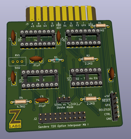
After the success with that previous PCB I designed and ordered, i decided to take a crack at something more complex. This time, an interposer to augment the Sanders 720 keyboard's feature set to allow me to have Control and Delete key functionality on something more robust than my homebrew prototype solution.
16 notes
·
View notes
Text
Empowering Electronics: The Rise of PCB Manufacturers in India
In the dynamic landscape of electronics, Printed Circuit Boards (PCBs) stand as the foundation upon which modern devices and technologies are built. As technology continues to advance, India has emerged as a significant player in the PCB manufacturing industry. This article explores the role and growth of PCB manufacturers in India, showcasing their contribution to the country’s technological progress.
The Role of PCBs in Electronics: Printed Circuit Boards are the intricate, interconnected networks that provide support and connectivity for electronic components within devices. From smartphones to medical equipment, virtually every electronic device relies on PCBs to function seamlessly. As technology evolves, the demand for more efficient, compact, and complex PCBs grows.
India’s PCB Manufacturing Landscape: India’s journey in the PCB manufacturing sector has been marked by substantial growth and advancements. With a growing electronics industry and an increasing emphasis on ‘Make in India,’ the country’s PCB manufacturers have risen to meet the demands of both domestic and international markets.
Advantages of PCB Manufacturing in India: Several factors contribute to India’s appeal as a best PCB manufacturing hub:
Skilled Workforce: India boasts a skilled pool of engineers, technicians, and designers, who contribute to the design, fabrication, and assembly of PCBs.
Cost Competitiveness: PCB manufacturing in India often offers a cost advantage compared to other regions, making it an attractive choice for global electronics manufacturers.
Technological Expertise: Indian PCB manufacturers are adept at incorporating cutting-edge technologies, such as flexible and high-density interconnect PCBs, to meet diverse industry needs.
Quality Standards: Many Indian PCB manufacturers adhere to international quality standards, ensuring the reliability and performance of the PCBs they produce.
Customization: PCB manufacturers in India are capable of producing customized solutions to meet the unique requirements of various industries.
Contributing to Technological Progress: The growth of PCB manufacturers in India aligns with the country’s aspirations of becoming a technology-driven global leader. By offering high-quality PCBs for a range of applications, Indian manufacturers contribute to advancements in sectors like telecommunications, automotive, healthcare, and more.
Global Reach and Impact: India’s PCB manufacturers have expanded their reach beyond national borders. Their products are used in devices and systems around the world, underscoring India’s capabilities in providing solutions for diverse industries.
Conclusion: As electronics continue to evolve and transform our world, the role of PCB manufacturers becomes increasingly vital. In India, PCB manufacturing has evolved into a thriving industry that not only meets domestic demands but also contributes to global technological progress. With a skilled workforce, competitive pricing, and a commitment to quality, PCB manufacturers in India are paving the way for a more connected and innovative future.
0 notes
Text
#pcb#pcb manufacturer#united states#europe#switzerland#germany#advanced circuit#partnership#branding#contract#business#printed circuit board#ttm#scc
0 notes
Text

Multilayer PCBs offer enhanced functionality by incorporating multiple circuit layers into a single board. These versatile boards enable complex electronic designs, compact layouts, and signal integrity. Our multilayer PCBs are meticulously manufactured, meeting industry standards for various applications, including consumer electronics, telecommunications, and aerospace technology.
Visit: https://sqpcb.com/products_category/multilayer-pcb
#Multilayer PCB#customized pcb boards#customize pcb#pcb board#aluminium pcb board#pcb china#printed circuit board#aluminum base pcb#circuit board#custom circuit boards
0 notes
Last Seen Blogs

justemz
JustEmz

drpepperzer0
Dr. Pepper Zero

bettymacs
BettyMacs

digitalmarketing448
Untitled

star-felled
it’s nothing too bad .ᐟ relatively speaking.