#but also produce electricity to interfere with electronics
Text
Slowly rotating Oracle in the Meat Marionette Au...

Au is a combo of mine & @phoenixcatch7 so go check out their Possessed Doll Au
#messy sketch#meat marionette au#batman#cryptid batfam#batman au#dc#dcu#oracle#batgirl#barbara gordon#sketch#idk i think her having a lot of arms and a chest cavity that stretches down would be cool#might replace the spikes with a bunch of wire-like tendrils that act similar to a jellyfish#but also produce electricity to interfere with electronics#god imagine if she could charge up some sort of biological emp thing with her wings#idk just thinking
79 notes
·
View notes
Photo
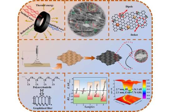
Electrospun nanomaterial offers great protection against electromagnetic interference
Engineers have employed "electrospinning," a new technique of manufacturing nanomaterials, to produce a novel fabric that offers high performance protection against electromagnetic interference, a phenomenon that can result in electronic device malfunction and at high levels of exposure can harm human health.
The technique is described in a paper published in Nano Research on December 31, 2022.
Electric and magnetic fields generated by electrical equipment can negatively interfere with digital systems either internally or externally. Such disruption can result in dangerous malfunctions if such devices are operating close to each other, particularly in the case of transportation or medical equipment such as pacemakers and insulin pumps. This interference can not only affect electronic devices, but at very high levels over short periods, it can also put at risk human biology, which in part makes use of bioelectromagnetic processes.
For all these reasons, a great deal of effort goes into shielding people, devices and parts of devices from electromagnetic interference. To avoid making devices—particularly wearable ones—overly bulky and heavy, such shielding also needs to be lightweight and flexible.
Read more.
#Materials Science#Science#Electrospinning#Nanotechnology#Electromagnetics#Composites#2D materials#MXenes
19 notes
·
View notes
Text
Electrons can be waves?
The double-slit experiment tells us that an Electron can move as both a particle AND a wave. But what if that's not the whole story?
When we turn off the lights in the double-slit experiment (And I'm stating this because it's something Niel DeGrasse Tyson said.) We see the wave pattern. But not if we try to view it in an environment with the lights on.
What is happening here?
Well; old auto-mechanic logic states the following old wives tale; "Current actually moves on the outside of a wire."
This is something that mechanics have noted at nighttime while doing repairs and watching the electricity from the alternator go through the large cables that power a cars internal electronics.
Because of the electric flow in the cable; electrons ALSO move on the outside of the cable AND produce light that you can see when the lights (the Sun) are off.
This is the wave. This means that electrons produce light, and that light creates the wave (or the interference pattern) that we see during the experiment.
It's not the electrons themselves; it's the light.
Now, when we say light can behave as a wave AND a particle; What they really mean is that the measurement devices can record the light beam (and resulting wave) as if it were a particle. (Or in the same exact manner as a particle)
And so we have this dichotomy here; resulting from how we talk about our measurements that makes a rational person infer that they're both particles and waves at the quantum scale when they're really not.
0 notes
Text
Choosing the Right Inverter: A Deep Dive into Sine Wave and Square Wave Technologies
In the quest for uninterrupted power and the comfort it brings to our daily lives, the modern homeowner faces a myriad of choices. Among these, selecting the right type of inverter for one's home stands out as a crucial decision. This article delves into the fundamental differences between sine wave and square wave inverters, offering insights into how these technologies impact your home energy solutions. Drawing from the extensive expertise of Okaya, a leader in the UPS/inverter industry, we uncover the nuances that could guide you to make an informed decision tailored to your household's needs.
Sine Wave Vs Square Wave Inverter: Differences You Must Know
Electricity not only powers our homes but also enriches our lives with convenience and efficiency. However, with the increasing frequency of power outages, the reliance on a dependable power backup solution has never been more critical. Here, the choice between sine wave and square wave inverters emerges as a significant consideration, impacting the quality of life and the longevity of household appliances.
The Fundamentals
1. Supported Appliances
Square Wave Inverters: These devices cater to basic, motor-driven appliances and are a cost-effective option for powering items such as fans and lighting fixtures. Their simplicity, however, limits their compatibility mainly to less sensitive appliances.
Sine Wave Inverters: Okaya's Ultra Pure series exemplifies the versatility and capability of sine wave inverters, supporting a wide range of devices from high-end electronics to delicate medical equipment. These inverters provide a safeguard for smooth operation and protect against potential damage.
2. Power Waveform
The essence of their difference lies in the type of power waveform each inverter produces. Sine wave inverters offer a smooth, consistent output that closely resembles the electrical grid's supply, ensuring compatibility with nearly all household devices. Square wave inverters, with their abrupt power transitions, cater to more basic needs but may introduce compatibility issues with more sophisticated electronics.
3. Overall Safety and Noise Interference
Safety: Sine wave inverters, particularly those in the Ultra Pure series from Okaya, prioritize the safety and longevity of household appliances with their true sine wave output. In contrast, the uneven power output from square wave inverters may pose risks to more sensitive devices.
Noise: The operational noise is another aspect where sine wave inverters excel, operating quietly and suitable for indoor use. Square wave inverters, on the other hand, might emit a level of noise that could be intrusive in home settings.
The Okaya Advantage
Okaya stands out in the inverter market with its commitment to quality, innovation, and understanding of modern household needs. From the energy-efficient Smart Wave series, based on Quasi Sine Wave technology, to the Ultra Pure series catering to high-end electronics with True Sine Wave output, Okaya addresses a broad spectrum of energy solutions. Their Hi-Capacity UPS options further emphasize the brand's dedication to robust, uninterrupted power for both residential and commercial settings.
In Conclusion The journey to choosing the right inverter for your home is paved with considerations of appliance compatibility, safety, noise levels, and the overall quality of power supply. With the insights into the differences between sine wave and square wave inverters, courtesy of Okaya's deep industry knowledge, homeowners are better equipped to make choices that align with their energy needs and lifestyle preferences. Okaya's range of inverters not only stands testament to its commitment to innovation and reliability but also assures homeowners of a seamless, uninterrupted power supply, ensuring a lifestyle unhampered by power disruptions.
0 notes
Text
Bhagyadeep Cables: Revolutionizing Automotive Connectivity with Advanced Wiring Harness Solutions
In the dynamic world of automotive engineering, where innovation and reliability are paramount, the role of wiring harnesses cannot be overstated. Serving as the nervous system of modern vehicles, wiring harnesses ensure seamless communication between various electronic components, powering everything from engine control systems to entertainment consoles. In this domain of automotive connectivity, Bhagyadeep Cables emerges as a pioneering force, renowned for its cutting-edge wiring harness solutions that drive efficiency, safety, and performance in vehicles worldwide.
Precision Engineering for Optimal Performance:
Bhagyadeep Cables epitomizes precision engineering, crafting automotive wiring harnesses with meticulous attention to detail and unwavering quality standards. Utilizing state-of-the-art technology and advanced manufacturing processes, their team of skilled engineers designs harnesses that meet the exact specifications of each vehicle model. From ensuring proper wire gauges to optimizing routing for minimal interference, Bhagyadeep Cables' wiring harnesses are engineered to deliver optimal performance under the most demanding conditions.
Customized Solutions for Every Application:
Recognizing the diverse needs of the automotive industry, Bhagyadeep Cables offers a comprehensive range of wiring harness solutions tailored to specific applications and requirements. Whether it's a compact city car, a rugged off-road vehicle, or a luxurious sedan, they provide customized harnesses that integrate seamlessly with the vehicle's architecture. By collaborating closely with automotive manufacturers, Bhagyadeep Cables delivers harnesses that not only meet technical specifications but also enhance functionality and aesthetics.
Innovation Driving Progress:
Innovation is at the core of Bhagyadeep Cables' DNA, driving continuous improvement and advancement in automotive wiring harness technology. They invest in research and development initiatives to stay ahead of industry trends and anticipate the evolving needs of automotive OEMs. By incorporating the latest materials, design methodologies, and manufacturing techniques, they develop innovative harness solutions that optimize performance, reliability, and cost-effectiveness, setting new benchmarks for excellence in the automotive industry.
Stringent Quality Control for Unparalleled Reliability:
Quality is non-negotiable at Bhagyadeep Cables, and they uphold the highest standards of excellence and reliability in every wiring harness they produce. Rigorous testing protocols, adherence to industry standards, and certifications ensure that each harness meets or exceeds the stringent requirements of automotive manufacturers. From conducting electrical conductivity tests to evaluating resistance to temperature extremes and vibration, Bhagyadeep Cables' wiring harnesses undergo comprehensive scrutiny to ensure unparalleled reliability on the road.
Commitment to Safety and Durability:
Safety is paramount in automotive design, and Bhagyadeep Cables prioritizes the safety and durability of their wiring harness solutions. They utilize materials that are resistant to abrasion, heat, and chemical exposure, ensuring long-term durability and protection against environmental factors. By incorporating features such as strain relief and insulation shielding, they mitigate the risk of electrical faults and ensure the integrity of critical vehicle systems, enhancing overall safety for drivers and passengers alike.
Driving Automotive Excellence:
As automotive technology continues to evolve at a rapid pace, the role of wiring harnesses in enabling innovation and connectivity becomes increasingly vital. In this ever-changing landscape, Bhagyadeep Cables remains at the forefront, driving automotive excellence with its advanced wiring harness solutions. Through precision engineering, customized solutions, innovation, stringent quality control, and a commitment to safety and durability, they continue to shape the future of automotive connectivity, powering vehicles that inspire confidence and performance on the road.
In conclusion, Bhagyadeep Cables stands as a trailblazer in the realm of automotive wiring harness solutions, delivering excellence and innovation that propel the automotive industry forward. With a dedication to precision engineering, customization, innovation, quality assurance, and safety, they remain the preferred partner for automotive manufacturers seeking reliable wiring harness solutions that meet the demands of today's vehicles and drive progress for tomorrow's mobility.
0 notes
Text
Navigating Regulatory Frameworks in the Pure Nickel Wire Market
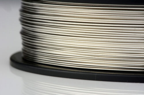
Pure Nickel Wire: Critical Component for Electrical and Electronics Industry
Introduction to Pure Nickel Wire
Pure nickel wire is a specialty electrical conducting material composed solely of nickel metal. With its unique conductivity and corrosion resistance properties, pure nickel wire finds wide application in industrial equipment, electronics, and other specialty uses. Let's take a closer look at the characteristics and applications of this important conducting material.
Physical and Electrical Properties
Pure nickel wire has several key physical properties that make it well-suited for specialized conducting applications. It has a silvery-white metallic appearance and is known for its high tensile strength, allowing it to withstand stresses without failure. Electrically, pure nickel has excellent conductivity, yielding a resistivity of around 6.99 μΩ·cm. It maintains this conductivity even at elevated temperatures up to around 300°C before declines set in. Moreover, pure nickel wire is non-magnetic, an important attribute for applications where magnetic properties could interfere. With a density of 8.9 g/cm3, it also weighs significantly more than other conductor metals like copper or aluminum.
Corrosion Resistance
One of pure nickel's most valued qualities is its corrosion resistance. It forms a passive oxide layer that protects the underlying metal from rusting or degrading when exposed to air, water, or various chemical environments. Thispassive layer regeneration even after damage occurs. As a result, pure nickel wire can withstand harsh, corrosive conditions where other metals would deteriorate quickly. Its resistance to seawater, acids, alkalis and various industrial chemicals make it well-suited for environments requiring corrosion protection.
Applications in Industry
Given its unique combinations of conductivity, strength and corrosion resistance, pure nickel finds wide use in industrial and specialty applications. Some key uses of pure nickel wire include:
- Cathode materials in alkaline batteries: Pure nickel provides the cathode for popular alkaline batteries due to its combinat ion of electrochemical properties.
- Heating elements: Thin nickel wires are woven into resistance heating cables, mats and other components for industrial heating processes requiring corrosion immunity.
- Solar cell contact wires: Ultra-thin nickel wires connect the light-absorbing elements in solar photovoltaic cells.
- Electrical contacts: Commutator segments and slip rings in motors and generators often use nickel for its self-lubricating surface oxidation layer.
- Welding electrodes: The corrosion resistance of nickel electrodes prevents weld contamination in industrial joining.
Development of High-Purity Variants
With the rise of microelectronics, demands have grown for ultra-high purity nickel wire able to meet stringent cleanliness thresholds. Producers have risen to the challenge by creating refining and wire drawing processes achieving 99.999% or higher purity levels. Variants include electrolytically refined "E-wire" for semiconductor applications and chemical vapor deposition-grade "CVD wire" fabricated at the molecular level with virtually no contaminants down to atomic levels. These high-purity wires enable innovations like miniaturized electronics, touchscreens, sensors and other precision devices.
Conclusion
In summary, pure nickel wire stands out as a premium electrical conductor for demanding applications. Its strength, conductivity and corrosion resistance have made it mission-critical in established industries while also enabling cutting-edge technologies. Continued process advancements aim to expand nickel wire's potential through ever higher purity levels and novel alloy variants. Given its versatility filling niche needs, pure nickel seems poised to remain a workhorse material supporting innovation well into the future.
0 notes
Text
Standard Earth Bars
Introduction:
In the realm of electrical engineering, ensuring safety and reliability are paramount concerns. Grounding systems play a critical role in maintaining electrical safety, and standard earth bars are fundamental components in these systems. In this article, we delve into the importance of standard earth bars, their functionality, and their significance in electrical installations, with a focus on Nexus Copper Pvt. Ltd's perspective.
Understanding Standard Earth Bars:
Standard earth bars, also known as grounding bars or earth bonding bars, are conductive devices used to create a connection between various grounding conductors and the grounding electrode system. They serve as central points for the termination of grounding conductors from electrical equipment, providing a low-resistance path to earth.
Functionality and Importance:
The primary function of standard earth bars is to ensure proper grounding and bonding within electrical installations. By establishing a reliable connection to the earth, these bars help dissipate excess electrical current, mitigate the risk of electrical faults, and protect personnel and equipment from electric shock hazards. They also aid in minimizing electromagnetic interference (EMI) and maintaining signal integrity in sensitive electronic systems.
Standard earth bars are essential in various applications, including industrial facilities, commercial buildings, data centers, telecommunications infrastructure, and residential settings. They are particularly crucial in environments where electrical equipment is prone to high fault currents or where sensitive electronic devices require protection against transient voltage surges.
Nexus Copper Pvt. Ltd's Contribution:
As a leading manufacturer and supplier of copper products,Nexus Copper Pvt. Ltd recognizes the critical role of standard earth bars in electrical safety and performance. Our company specializes in producing high-quality copper earth bars that meet industry standards and specifications.
Nexus Copper Pvt. Ltd's standard earth bars are meticulously designed and manufactured using premium-grade copper materials, ensuring excellent conductivity, corrosion resistance, and durability. Our products undergo rigorous quality control measures to guarantee reliability and compliance with international standards.
Moreover, Nexus Copper Pvt. Ltd offers a comprehensive range ofstandard earth bars in various sizes, configurations, and finishes to cater to diverse customer requirements. Whether for industrial, commercial, or residential applications, our earth bars are engineered to deliver optimal performance and long-term reliability.
Conclusion:
standard earth barsplay a critical role in ensuring electrical safety, reliability, and performance in various applications.Nexus Copper Pvt. Ltd, with its commitment to quality and innovation, provides premium-grade standard earth bars that meet the highest standards of excellence. By investing in reliable grounding solutions, organizations can safeguard their personnel, equipment, and assets against the risks posed by electrical faults and ensure uninterrupted operation of their electrical systems.
0 notes
Text
What are the disadvantages of an induction stove top?
Induction stove tops offer many benefits, such as faster cooking times, precise temperature control, and energy efficiency. However, they also come with some disadvantages:
Initial Cost: Induction stove tops tend to have a higher upfront cost compared to traditional gas or electric stoves. The technology involved in induction cooking can make these appliances more expensive to purchase initially.
Compatibility with Cookware: Induction stoves require compatible cookware made from ferrous materials like cast iron or stainless steel. Cookware made from aluminum, copper, or glass will not work on induction stoves unless they have a magnetic bottom. This limitation may require users to invest in new cookware.
Potential for Electromagnetic Interference: Induction stoves generate electromagnetic fields to heat the cookware. While these fields are generally safe, they can interfere with certain electronic devices like pacemakers or hearing aids. Individuals with such devices may need to take precautions or avoid using induction stoves altogether.
Noise: Some users find that induction stoves produce a faint humming sound during operation. While not excessively loud, this noise may be noticeable, especially in quiet kitchens.
Power Supply Requirements: Induction stoves require a dedicated power supply with specific voltage and amperage requirements. If your kitchen is not already equipped with the necessary electrical setup, installation costs may increase.
Despite these disadvantages, many users find that the benefits of induction cooking outweigh the drawbacks, particularly in terms of efficiency and cooking performance.
#induction#stove#kitchen#modular kitchen#modern kitchen#modern living#interor design#home decor#cooktop#induction stove
0 notes
Text
Types and Functions of Diodes - A Comprehensive Guide
Email: [email protected]
WhatsApp & Wechat: +86 18038197291
www.xygledscreen.com
Diodes are a crucial electrical component. They appear in various items, including computers, televisions, radar circuits, power supply systems, and communications systems. Understanding diodes can help one understand why it is such an essential component.
Check out this comprehensive guide concerning the function of diodes. It will provide insight into what diodes are, how diodes work, their benefits and drawbacks, their various types, and their applications.
What Is a Diode?
A diode is a one-way switch in a circuit. It allows electrical current to move in a specific direction and prevents it from moving in the opposite direction. This device typically has two terminals. One is the positive terminal, the anode, and the other is the negative terminal, the cathode.
Many diodes consist of semiconductor materials, such as selenium. Semiconductors are substances with conductivity levels lower than conductors but higher than insulators. People often rate diodes by their current capacity, type, and voltage.
How Do Diodes Work?
The most common kind of diode is the semiconductor diode. It has a P-type layer of positively charged particles and an N-type layer of negatively charged particles. When these two layers come together, they create a PN junction.
A PN junction impacts the flow of current. The positively charged particles in the P-type layer of the junction are attracted to the negatively charged particles in the N-type layer. Their attraction creates a barrier.
An electrode attached to the P-type layer is an anode, and one attached to the N-type semiconductor is a cathode. When connected to a power source, the current will flow from the anode to the cathode. It will not flow from the cathode to the anode.
What Are the Advantages of a Diode?
There are several advantages associated with using diodes. First, they prevent electrical circuits from sustaining damage from overcurrents, short circuits, and overvoltages. Second, they can change alternating current (AC) to direct current (DC).
Third, diodes decrease power losses within an electrical circuit. Fourth, diodes can lessen electromagnetic interference (EMI). Lastly, you can execute logic operations with diodes because they can produce logic gates.
What Are the Disadvantages of a Diode?
Though diodes can protect electrical circuits, their efficiency is comparatively low. Their voltage drop is ~0.7V, so they use power even when there is no current flow. The low efficiency makes diodes unideal for electrical circuits that need high efficiency, such as solar cells.
Diodes are susceptible to heat damage. They can experience an overload of current, resulting in damage or failure. A drawback of semiconductor diodes is that they cannot handle high reverse voltage. Also, semiconductor diodes have high noise levels at high frequencies.
What Are the Different Types of Diodes?
Several types of diodes are available on the market, such as PN junction diodes, photodiodes, rectifiers, PIN diodes, and light-emitting diodes (LEDs).
A PN junction diode, also known as a general purpose diode, has two terminals, the anode and cathode. The current in this diode moves in one direction, from the anode to the cathode. This type of diode has a P-type layer with positive ions and an N-type layer with negative electrons. You can find these diodes in automotive, computer, and communication devices.
A photodiode, called a light detector or photo-detector, uses light energy to yield a current. This device has two electrodes and a radiation-sensitive junction. It is an optoelectronic component that supports a reverse current that changes with illumination. Photodiodes usually consist of materials such as germanium and silicon. People often employ them to detect and convert optical power.
A rectifier takes in AC that has, on average, zero volts. It converts AC to DC. The DC the rectifier yields has a net value of more than zero. Rectification is the name of this AC to DC process. The diode in the rectifier has an anode and cathode and sustains a current that flows in a single direction.
A PIN diode features three semiconductor regions. One of the regions is a p-type semiconductor, and the other is an n-type one. The layer that is between the p-type and n-type layers is the intrinsic region. This region is large and undoped. The p-type and n-type regions have impurities to facilitate ohmic contacts.
A light-emitting diode gives off light radiation via electroluminescence. It has a PN junction and serves as an illuminator or visual indicator. LEDs on the market can support infrared, visible, and ultraviolet light. Plenty of industries use LEDs. You can find them in automobiles, aircraft carriers, televisions, and lamps.
What Are the Common Applications of Diodes?
People use diodes in a variety of ways. They appear in devices found in industrial, commercial, and residential settings.
Many use diodes for rectification. Converting AC to DC helps because it stops voltage spikes. Thus, you will find diodes in items such as surge protectors.
Diodes appear in logic gates because they can enact digital logic functions. You will find diodes in digital electronics, such as computer processors.
Diodes work well for radio demodulation, also known as signal demodulation. This process isolates signals from a supply of current. People use diodes to get radio signals from a carrier. Look at a present-day radio circuit. A diode will likely be there.
Those who need to measure or manipulate light frequently employ diodes to achieve their desired results. Photodiodes can measure light intensity, and LEDs can function as a light source because they appear in illumination technology, such as light bulbs.
Voltage multiplication is another process that people use diodes to perform. The diode, plus a capacitor, will use AC with a low voltage value and multiply it, increasing its voltage. Many electric devices, such as power supplies, feature voltage multipliers.
In conclusion, diodes are vital electrical devices with strengths, limitations, and multiple applications. There are many types of diodes, including rectifiers, photodiodes, and LEDs. Some use diodes on occasion for special electrical applications. Others use them daily because they appear in household appliances, computers, and communication devices. Many tools, systems, and processes could not exist without the assistance of diodes.
0 notes
Text
Global Automotive Shielding Market Analysis 2024 – Estimated Market Size And Key Drivers
The Automotive Shielding by The Business Research Company provides market overview across 60+ geographies in the seven regions - Asia-Pacific, Western Europe, Eastern Europe, North America, South America, the Middle East, and Africa, encompassing 27 major global industries. The report presents a comprehensive analysis over a ten-year historic period (2010-2021) and extends its insights into a ten-year forecast period (2023-2033).
Learn More On The Automotive Shielding Market:
https://www.thebusinessresearchcompany.com/report/automotive-shielding-global-market-report
According to The Business Research Company’s Automotive Shielding, The automotive shielding market size has grown strongly in recent years. It will grow from $16.02 billion in 2023 to $17.14 billion in 2024 at a compound annual growth rate (CAGR) of 7.0%. The growth in the historic period can be attributed to electromagnetic interference (emi) concerns, regulatory compliance, consumer safety concerns, increased vehicle connectivity, globalization of automotive supply chains.
The automotive shielding market size is expected to see strong growth in the next few years. It will grow to $22.58 billion in 2028 at a compound annual growth rate (CAGR) of 7.1%. The growth in the forecast period can be attributed to lightweighting initiatives, autonomous vehicles, electrification of vehicles, advanced driver assistance systems (adas), connectivity in electric vehicles, increased vehicle complexity. Major trends in the forecast period include integrated shielding designs, customization for electric vehicles, flexible and conformable shielding, multi-layer shielding, 3d printing for customized shielding.
Increasing vehicle production is expected to propel the growth of the automotive shielding market going forward. A vehicle is a machine with an engine and wheels that transports people or cargo. Due to rapid urbanization and the expansion of global auto manufacturers, vehicle production has been on the rise in recent years. Since automotive shielding is used in electronic components of vehicles, increased vehicle production results in an increased demand for automotive shielding. For instance, according to the European Automobile Manufacturers' Association (ACEA), a Belgium-based group in the automobile industry, in 2021, 79.1 million motor vehicles were produced globally, a 1.3% increase from 2020. Therefore, growing vehicle production is driving the growth of the automotive shielding market.
Get A Free Sample Of The Report (Includes Graphs And Tables):
https://www.thebusinessresearchcompany.com/sample.aspx?id=7520&type=smp
The automotive shielding market covered in this report is segmented –
1) By Shielding Type: Heat Shielding, EMI Shielding
2) By Material Type: Metallic, Non-Metallic
3) By Vehicle Type: Passenger Car, Light Commercial Vehicle, Heavy Commercial Vehicle
Technological advancements have emerged as the key trend gaining popularity in the automotive shielding market. Major companies operating in the automotive shielding sector are focused on introducing new technologies to strengthen their market position and meet customer demand. For instance, in June 2022, Bourns, Inc., a US-based manufacturer and supplier of electronic components for power, protection, and sensing solutions, announced a new AEC-Q200-compliant, automotive-grade semi-shielded power inductor series that features a high operating temperature range from -40 °C up to 150 °C. The Bourns Model SRN8040HA Series is constructed using the company's advanced magnetic silicon-based coating technology, which offers superior magnetic shielding while also enabling higher operating temperatures.
The automotive shielding market report table of contents includes:
Executive Summary
Market Characteristics
Market Trends And Strategies
Impact Of COVID-19
Market Size And Growth
Segmentation
Regional And Country Analysis
.
.
.
Competitive Landscape And Company Profiles
Key Mergers And Acquisitions
Future Outlook and Potential Analysis
Contact Us:
The Business Research Company
Europe: +44 207 1930 708
Asia: +91 88972 63534
Americas: +1 315 623 0293
Email: [email protected]
Follow Us On:
LinkedIn: https://in.linkedin.com/company/the-business-research-company
Twitter: https://twitter.com/tbrc_info
Facebook: https://www.facebook.com/TheBusinessResearchCompany
YouTube: https://www.youtube.com/channel/UC24_fI0rV8cR5DxlCpgmyFQ
Blog: https://blog.tbrc.info/
Healthcare Blog: https://healthcareresearchreports.com/
Global Market Model: https://www.thebusinessresearchcompany.com/global-market-model
0 notes
Text
Essential Role of EMI/EMC Studies for Electrical Device Compatibility
From smartphones to medical equipment and automobiles, these devices rely on intricate electronic systems to function efficiently. However, the proliferation of electronic devices has also brought about a growing concern: electromagnetic interference (EMI) and electromagnetic compatibility (EMC). In this blog, we will explore the significance of EMI/EMC studies and why they are crucial for ensuring the proper functioning and safety of electronic devices.
Understanding EMI and EMC
Electromagnetic Interference (EMI) refers to the disturbance generated by one electronic device that affects the normal operation of another nearby device. These disturbances can manifest as electromagnetic radiation, radiofrequency interference (RFI), or conducted interference. EMI can result in malfunctions, data corruption, or even safety hazards.
Electromagnetic Compatibility (EMC), on the other hand, is the ability of electronic devices to operate efficiently in the presence of EMI and not produce excessive interference themselves. EMC ensures that devices can coexist and function as intended within their electromagnetic environment.
The Importance of EMI/EMC Studies
Device Reliability: EMI can lead to erratic behavior or malfunctioning of electronic devices. EMI/EMC studies help identify potential sources of interference and mitigate them during the design and testing phases, ensuring the reliability of the device.
Compliance with Standards: Regulatory agencies and standards organizations (e.g., FCC, CE marking) have strict guidelines regarding EMI/EMC. Manufacturers must adhere to these standards to bring their products to market legally. EMI/EMC studies help ensure compliance, preventing costly delays or product recalls.
Safety: Some devices, such as medical equipment or avionics, must operate flawlessly to ensure user safety. EMI/EMC studies identify potential safety risks posed by electromagnetic interference and provide solutions to mitigate them.
Avoiding Data Corruption: In sectors like telecommunications and data centers, data integrity is critical. EMI can corrupt data signals and disrupt communication. EMI/EMC studies help maintain data integrity and prevent communication breakdowns.
Reducing Liability: Failure to address EMI/EMC issues can lead to liability concerns if interference from a device causes harm or damage to other equipment or systems. Conducting EMI/EMC studies mitigates these risks.
Interference Prevention: In densely populated areas with numerous electronic devices, EMI can become a significant issue. EMI/EMC studies help prevent interference between neighboring devices, improving overall performance.
Cost Savings: Identifying and addressing EMI/EMC issues during the design phase is more cost-effective than making modifications after production. Early detection and mitigation can save both time and money.
Global Market Access: EMI/EMC compliance is often a prerequisite for entering international markets. Products that have undergone EMI/EMC testing and comply with relevant standards can access a broader customer base.
Conclusion
In a world driven by electronic devices and interconnected technologies, ensuring EMI and EMC compatibility is of paramount importance. EMI/EMC studies play a vital role in identifying potential sources of interference, preventing malfunctions, ensuring safety, and facilitating compliance with regulatory standards. By conducting these studies during the design and development phases, manufacturers can produce reliable and safe electronic devices that not only meet the demands of the market but also contribute to a seamless and interference-free user experience. In essence, EMI/EMC studies are a cornerstone of modern electronics, guaranteeing compatibility in an increasingly electrified world.
0 notes
Text
Withstand Voltage Test (Dielectric Voltage Withstand Test): Principles, Purposes, and Applications
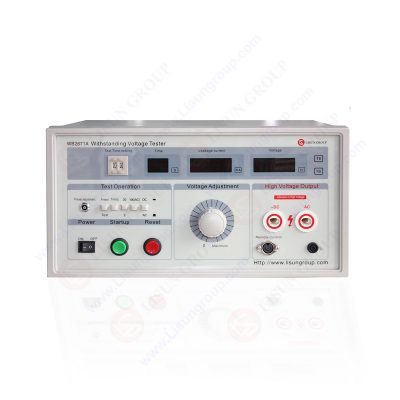
The principle of withstand voltage test:
Withstand voltage test, also is called dielectric voltage withstand test, is a testing method for measuring the conducting performance of a device and its resistance to high voltage charge damage, mainly used for detecting electrical safety. It can be used for both regular circuit products and prototype for new development, providing guarantee for further safe usage. Withstand voltage test uses high voltage pulses to test the insulation performance of the tested system to see whether short circuits or overloads will occur. The settings of test conditions will directly influence the accuracy and reliability of the test results. Therefore, prior to testing, parameters should be studied and calculated carefully to ensure test accuracy.
What is hipot testing used for?
Hipot testing is a non-destructive test used to check the insulation capability of tested products under instantaneous high voltage environment. This test requires keeping a certain degree of high voltage in fixed time in order to ensure the strong and effective insulation performance of tested equipment. Besides, withstand voltage test can also detect some defects in the manufacture process of the instrument, such as deficient creepage distance and electric clearance, etc. Withstand voltage test is an important test which can quickly and accurately determine the capability of tested equipment against instantaneous high voltage in order to ensure the security and reliability of the tested equipment.
With the development of science and technology, the new type withstand voltage testers have enough of source voltage and load regulation rate, so the withstand voltage testers with capacity of 500VA have been eliminated from the new safety standards. In addition, this has brought threats to the operators’ operations, under different test requirements and large quantities of test processes, the withstand voltage testing equipment requires stronger performance, and the testers based on transformer and voltage regulator are no longer applicable.
Now, the new type withstand voltage testers can be divided into two types: one is composed of single-chip computer as the core, digital control waveforms combined with linear power amplifier; the other type is composed of single-chip computer core and SPWM (sinusoidal pulse width modulator) pulse generator , combined with IGBT (insulated gate bipolar transistor) pulse power amplifier, making it have stronger test capabilities. Not only it meets the requirements of different standards and large quantities of test processes, but it can also detect potential problems of the tested articles’ insulation performance such as arc, creepage and flash-over better. Thus, the new generation of withstand voltage testers are rapidly popularizing, continuously improving the safety performance of electronic equipment.
The withstand voltage test equipment has a complex structure, and its reliability and anti-interference ability depend on the design and quality of the electronic components. It has small distortional waveform, variable output frequency (50/60Hz), wide output voltage adjustment range and high control accuracy, can produce stable output voltage within the power range, not affected by load change, and can reach 500W output power. Besides, this instrument can also achieve automatic protection, and it can still operate safely even if there is no voltage output, which can help detect potential problems of the tested articles’ insulation performance such as arc, creepage and flash-over.
In addition, withstand voltage tester can achieve various standard requirements through the software, such as step up voltage, timed up voltage, constant speed up voltage, etc., and can also conduct breakdown point analysis, with breakdown protection and high display resolution leakage current display, which is particularly suitable for testing electrical appliances or components with high standards. Moreover, it is stable when working, can be networked with computers, thus realizing test statistical and sorting work, and can continuously test the tested articles.
The withstand voltage testing equipment is an important electronic testing equipment, which is mainly composed of AC (DC) high voltage power supply, timer controller, test circuit, display circuit and alarm circuit, etc. The working principle of this equipment is to measure the leakage current of the tested instrument by outputting the high voltage test, and to compare it with the preset judgment current. If the detected leakage current is lower than the predetermined value, the instrument is tested OK; while if the detected leakage current is greater than the preset judgment current, the test voltage will be cut off instantaneously, accompanied by sound and light alarm, and finally to determine the withstand voltage strength of the tested instrument. The technical specifications of this equipment mainly include output voltage and preset cut-off current, while the analog indicator type withstand voltage tester is generally characterized by its voltage magnitude in the form of allowable error.
Lisun Instruments Limited was found by LISUN GROUP in 2003. LISUN quality system has been strictly certified by ISO9001:2015. As a CIE Membership, LISUN products are designed based on CIE, IEC and other international or national standards. All products passed CE certificate and authenticated by the third party lab.
Our main products are Goniophotometer, Integrating Sphere, Spectroradiometer, Surge Generator, ESD Simulator Guns, EMI Receiver, EMC Test Equipment, Electrical Safety Tester, Environmental Chamber, Temperature Chamber, Climate Chamber, Thermal Chamber, Salt Spray Test, Dust Test Chamber, Waterproof Test, RoHS Test (EDXRF), Glow Wire Test and Needle Flame Test.
Please feel free to contact us if you need any support.
Tech Dep: [email protected], Cell/WhatsApp:+8615317907381
Sales Dep: [email protected], Cell/WhatsApp:+8618117273997
Read the full article
0 notes
Text
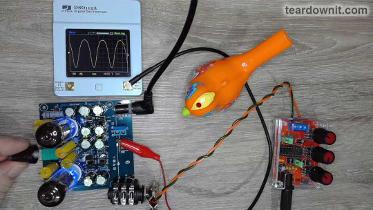
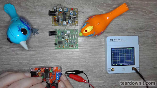
DIY functional oscillators

Signal distortion induced by electronic devices, primarily amplifiers, could be either undesirable or useful.
When we play back an audio recording, we want it to sound as close to the original as possible. Or sometimes, we want to add just a smidge of tube distortion.
On the other hand, magnetic recording on tape and mechanical recording on vinyl, by their nature, significantly alter the sound; therefore, distortions are deliberately added into the circuits of recorders and playback equipment so that, in the end, the resulting audio signal turns out to be indistinguishable from what has been recorded.
In addition, volume controls are equipped with loudness compensation to account for human hearing abilities.
Mobile pocket audio devices have tiny speakers, and their power amplifiers are specifically designed to add bass and limit treble so that the sound is deeper and less squeaky.
Multi-way speaker systems have filters, and sometimes even separate amplifiers, that slice the sound signal into frequency bands for each dedicated speaker: subwoofer, low-frequency, mid-frequency, and tweeter. These can also be considered deliberately created distortions.
Finally, processing an electric guitar signal requires numerous fine-tuned distortions. They form a wonderful guitar tone. But if we simply plug the best electric guitar into a hi-fi amplifier, we'll be disappointed.
One can also identify a malfunction by the specific distortions of the signal and, by tracking the signal flow, specify the location of the malfunction in a complex circuit.
A device that allows you to see distortions is called an oscilloscope. But having an oscilloscope is not enough; we will also need a standard waveform signal generator. Today, we will assemble three such generators.
So-called standard waveforms are sine, triangle, and square. Devices that generate such signals are called function generators.
A sine wave is the simplest signal, but it is the most difficult to create without an LC resonant tank, using only RC circuits. A pure sine wave oscillates one frequency; it is needed to determine the harmonics the circuit adds to the signal.
For example, in this image from the post about the tube amplifier, we see that the upper half-wave is wide and rounded, and the lower half-wave is narrow and pointy. This indicates the presence of a second harmonic, which makes tube amplifiers sound so beautiful.

A triangular waveform could be created by a ramp voltage generator. Such a signal allows one to see nonlinear distortions as lines bend on the oscilloscope screen.

Bending them a certain way brings the triangle line closer to a sinusoid. This is exactly how the function generators on microchips that we are studying today are designed.
An ideal square wave consists of vertical and horizontal lines. Looking at the flow of such a signal, one can see the frequency-dependent deviations, interference, and parasitic processes.
For example, a differentiating circuit with a time constant of an order of magnitude smaller than the period of the input signal creates a sharp peak at the beginning of the horizontal section.

And this is what the result of the operation of an integrating circuit with a time constant comparable to the signal period looks like.
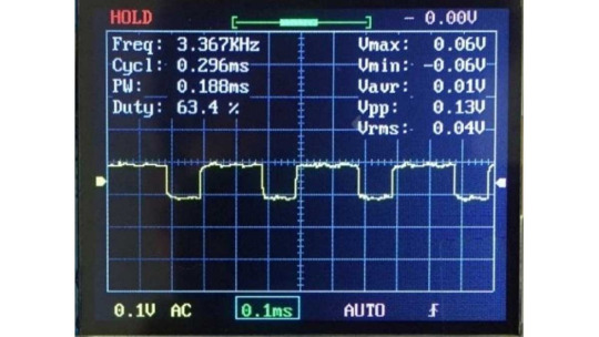
If the integrator time constant is noticeably smaller than the signal period, then only the leading edges become sloped, and the top part of the square wave remains flat. In this oscillogram, we see additional high-frequency interference.
Here, we see not just high-frequency noise but damping oscillations excited by sudden changes in the input signal. Such vibrations are called "ringing".
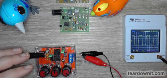
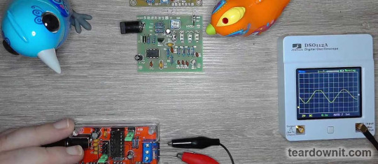
Function generator on the XR2206 chip
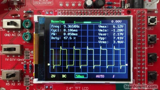
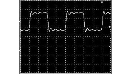
Our first generator can produce electrical oscillations with frequencies ranging from 1 Hz to 1 MHz. This is more than enough for an amateur's lab.
The 300 kHz square wave we have here is distorted not by the generator itself but by the DSO112A oscilloscope, whose analog bandwidth is 2 MHz.

At 20 kHz, the upper limit of the audible range, the square waveform appears almost perfect.
The generator volume knob allows one to crank it up to the limiter. This generator feature must be kept in mind, or the limitation may sometimes seem to occur in the circuit under study.

The 400 kHz sine wave looks great. Remember that this is 1/5 of the oscilloscope's bandwidth, so all the harmonics higher than the fifth won't pass through the oscilloscope's analog input.

This is a triangular waveform at a frequency of 130 kHz. The tops are slightly rounded, but the lines are straight. Everything looks as it should.
The generator circuit is elementary. Capacitors C1 and C2 together are a power filter. The square wave output is pulled up by resistor R1 to the power supply positive because it is an open collector output.
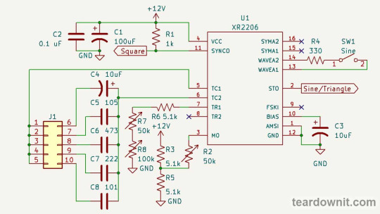
C4-C8 are timing capacitors, and J1 is their frequency range switch.
Timing resistance is made up of three series resistors. R8 is a coarse frequency setting, R7 is a fine setting, and R6 is a limiting resistor, so it cannot be zero.
The circuit has input 8 (TR2) for the second timing resistor. Pull pin 9 (FSKI) to the ground; input 8 (TR2) will become active. If input 8 is left disconnected or pulled to the power supply positive, then input 7 (TR1) is active.
This option allows one to instantly switch between two oscillation periods, which is helpful for frequency shift keying or pulse width modulation.
To get PWM, one needs to connect input 9 (FSKI) to output 11 (SYNCO). Then, the duty cycle will be determined by the ratio of the resistances connecting TR1 and TR2 to the ground, and the frequency will be determined by the sum of these resistances.
Pin 3 (MO) bias setting is the gain adjustment. It is the amplitude of the output signal and is tweaked with a variable resistor, R2.
Pins 13 and 14 (WAVEA1, WAVEA2) are used to form a sinusoid. Output 2 (STO) produces a triangle waveform if they are open. If those pins are connected through a resistor, there will be a sine wave. Its shape can be adjusted by changing the resistance R4.
Input 1 (AMSI) is intended for amplitude modulation. We don't use it in this scheme.
Output 10 (BIAS) is connected to the internal reference voltage source. To ensure its stability and the absence of any interference, a capacitor C3 is connected to it.
You can add a potentiometer to pins 15 and 16 (SYMA1 and SYMA2) and connect its wiper to the ground. Then, it will be possible to further adjust the symmetry of the sinusoid. Although, as we've seen, this is optional.
Function generator on the ICL8038 chip
The ICL8038 chip has much in common with the XR2206; it is also designed to create a function generator with minimum external components.
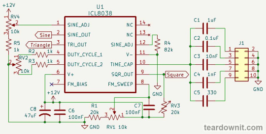
Like the XR2206, the ICL8038 has a timing capacitor on input 9 (TIME_CAP). We switch through five different capacitors to get five frequency ranges.
Square wave output 9 (SQR_OUT) for both microcircuits is an open collector. It needs to be pulled up to the positive power supply. ICL8038 has separate sine and triangle outputs: 2 (SINE_OUT) and 3 (TRI_OUT).
The ICL8038 has only one input for timing resistor 8 (FM SWEEP), so we won't be able to switch between resistors and get FSK.
But inputs 4 and 5 allow one to adjust the duty cycle of PWM. The resistances between these pins and the power supply positive, set by the position of wiper RV2, affect all three outputs.

Resistor RV4, the bias of input 1 (SINE_ADJ), tweaks the vertical symmetry of the sine wave. As we already know, this affects the harmonic series of the signal.

Simple function generator on NE555
If you do not have a specialized chip, a simple square, triangle, and sine wave generator can be assembled in many ways, for example, on a 555 timer.
We see an emitter follower on transistor Q1 at the device's output. It has a positive bias in the form of resistor R10. The input resistance of this stage is about 100 kOhm, so the voltage at the base of Q1 will be about half the supply voltage.

In the first position of the switch, rectangular pulses from the output of the 555 timers pass through series capacitors C4 and C5 and parallel capacitor C6. Resistor R3 is connected with C4, and R4 is connected in parallel with C6.
The result is a hybrid of a rectangle and a ramp with decent linearity. One can evaluate the distortion and parasitic oscillations it introduces by comparing the original waveform with what is produced in a particular circuit.
Next comes the integrator R5C7, after which crescent-shaped relaxation oscillations are obtained. The authors labeled this waveform a sawtooth or ramp, but it's more like shark fins.

After the second similar integrator, R6C8, a hybrid of a triangle and a sine wave is created: the tops are rounded, but the inclined sections are almost linear.

And finally, after the transistor stage on Q2, shunted by capacitor C9, we get an excellent approximation of a sinusoid. Resistor R8 provides base bias to Q2.

So we've seen what capacitors, resistors, and a transistor do to an electrical signal, and we learned how to build a simple generator with recognizable waveforms that can be used to study distortions in electrical circuits.
It is not that difficult to assemble a proper function generator on a special microcircuit. Still, it will definitely have more functions and better signal quality.
Professional-grade devices are, of course, more advanced, but they have a much higher price and substantially bigger dimensions. Unlike the three simple generators we've assembled and tested today, not every electronics enthusiast can afford them.
youtube
0 notes
Text
Debunking TEC Testing and Qualification in the World of Electronic devices
In tec testing of electronic devices, making certain products satisfy rigorous top quality, efficiency, and security criteria is paramount. The Telecommunication Design Center (TEC) in India stands as a pivotal entity in this landscape, playing a critical role in the testing and qualification of telecommunications equipment.
Recognizing TEC Certification
TEC Certification, regulated by the Division of Telecommunications (DoT) in India, verifies the conformity of telecom devices with vital technical requirements and specs. This certification makes sure that devices meet the requirements for interoperability, high quality, and security in the Indian telecommunications network.
Strenuous Checking Procedures
TEC Testing involves a detailed evaluation of telecommunications devices across numerous parameters. These tests encompass performance, electro-magnetic compatibility, electric safety and security, ecological influence, and extra. The assessments rigorously take a look at devices to ensure they align with TEC's strict requirements.
Key Aspects of TEC Testing
Capability Screening: Examining the performance and functionality of gadgets to verify their integrity and efficiency in real-world scenarios.
Electromagnetic Compatibility (EMC) Testing: Assessing the tool's capability to run effectively without triggering interference in the telecom network or various other digital devices.
Electric Safety And Security Evaluating: Guaranteeing tools fulfill security criteria to stop electrical threats, securing both customers and the network infrastructure.
Environmental Effect Assessment: Validating the tool's durability in different ecological conditions, such as temperature, humidity, and vibration.
The Importance of TEC Qualification
TEC Accreditation functions as a mark of quality and conformity, instilling self-confidence in customers, provider, and producers. It assures customers that the telecommunications equipment they utilize adheres to robust requirements, making certain seamless connectivity and safety.
Streamlining Item Development
For makers, obtaining TEC Qualification improves the item development procedure. It overviews them to create and generate tools that adhere to Indian telecommunications laws from the outset, preventing difficulties during release.
The Function in Telecommunication Development
TEC plays a crucial duty in advancing the telecommunications sector in India. By establishing and imposing standards, it adds to the growth, performance, and safety and security of telecommunication facilities throughout the nation.
Embracing Advancement and Adaptability
As innovation evolves, TEC constantly updates its criteria to fit advancements. This versatility urges advancement in the telecommunications industry while maintaining the stability of the network.
Final thought
TEC Testing and Accreditation form the foundation of guaranteeing telecom equipment's adherence to strict criteria in India. This strenuous procedure not only guarantees the quality and security of tools however also cultivates a robust and reliable telecommunication network. In the ever-evolving landscape of electronic devices, TEC Certification continues to be a crucial factor in driving innovation, securing customers, and advancing the nation's telecommunication
1 note
·
View note
Text
Innovative Solar Solutions
Solar energy entered the mainstream with the installation of solar panels on houses, but there are many more ways to harness its power. Read on to learn more about some of the neat innovations available and in development that utilize solar energy.
Grid-tie solar systems generate electricity during the daytime and send it to the public utility grid. The company then credits you for the power you produce.
Solar Panels
Solar power systems are a crucial tool for combating climate change and reducing dependence on fossil fuels. By capturing the sun’s energy and turning it into electricity, solar solutions panels provide a clean alternative to dirty fuels that are responsible for a range of environmental problems, including air pollution, acid rain, water shortages, rapidly filling waste disposal sites, and the destruction of wildlife habitat.
Solar panels are made up of photovoltaic cells that generate direct current (DC) electricity. When photons from the sun hit the cells, they knock electrons loose from their atoms. When metal conductors are attached to the positive and negative sides of the cell, the electrons flow through the circuit, much like a battery powers a light bulb.
A variety of solar panel technologies exist, including monocrystalline and polycrystalline silicon cells. Monocrystalline cells use single, pure crystals to create wafers that are then assembled into panels. Polycrystalline solar panels utilize multiple silicon molecules, which reduces efficiency but saves on manufacturing costs.
Solar Control Films
Solar control films are a passive solution to improve the thermal, luminous and energy performance of building glazing systems without facade alteration. They reduce extreme solar gains, control glare and moderate the amount of visible light and near infrared radiation transmitted through the window.
They are very thin polyester-based products coated and laminated with different types of metals. Their spectrally selective coatings enable less transmission of the sun’s harmful UV radiation and visible light while transmitting the desired range of near infrared heat.
These film coatings can be tinted in a variety of warm or cool shades and even mirrored to provide homeowners with aesthetic options that keep rooms bright and comfortable. They also help save energy by reducing the amount of air conditioning use during hot summer months, and they can significantly reduce heating energy usage in winter. Choosing the right window film depends on the needs and goals of each homeowner. These products are available for both residential and commercial buildings.
Window Tinting
Window tinting can be used to defend against harmful UV rays and mitigate solar heat, while also saving energy on your Phoenix or Mesa home’s utility bills. Unlike sun screens that obstruct views, window film solutions allow for unimpeded exterior visibility and are available in various shades to suit your preferences.
A popular solar window tint solution is CoolVu, which uses photochromic transitions to darken windows when it gets hot and lighten them when it’s cooler. This innovative technology can be triggered by natural sunlight or interior lighting and requires no maintenance.
CoolVu solar window tints reduce up to 99% of the sun’s cancer-causing UV rays and help extend the life of furniture, carpeting, wall coverings, paintings, and hardwoods. These tints are durable, resist fading, and won’t interfere with radio or phone signals. They offer a sleek appearance and reduce in-cabin temperatures by up to 45 degrees. They also won’t void your window manufacturer warranty.
Home Backup Generators
With power outages on the rise across the country due to natural disasters and weather-related events, a solar panel services generator is becoming an essential home investment. While traditional gas-powered generators use fossil fuel, solar-plusstorage systems like PWRcell capture and store electricity from either sunlight or the grid for backup power during power outages.
This enables homeowners to access clean, affordable electricity and reduce their electric bills even during times of peak demand. It also makes it easier to power up critical appliances during a short-lived outage, while the battery system recharges.
These systems have built-in transfer switches that disconnect your home from the grid during a blackout. They can also monitor power frequency to prevent unessential loads from drawing too much energy and tripping the breakers, making them more user-friendly than regular home generators. They’re also better for the environment, since they don’t emit any noxious fumes during operation. In addition to home storage, these systems can be used for portable applications like RVs and campers.
1 note
·
View note
Text
Investment Opportunities in the Microwave Monolithic Integrated Circuits Sector
The spintronics market is projected to reach a value of US$ 687.1 million in 2023, with a forecasted compound annual growth rate (CAGR) of 7.3% leading to a market size of US$ 1,394.2 million by 2033.
The introduction of spintronics technology has revolutionized the storage and processing of massive data, leading to increased market share. Further, the demand for spintronics is driven by its applications in hard drives, digital electronics, sensors, and more.
Spintronics utilizes the spin of electrons rather than their charges, enabling energy-efficient chips and memory-storage devices. Magnetic RAM (MRAM) has emerged as a prominent spintronics technology, offering large storage space and potentially replacing conventional RAMs.
Accelerate Your Success: Unlock the Secrets of the Spintronics Market – Download the Sample Report @
https://www.futuremarketinsights.com/reports/sample/rep-gb-5912
Spintronics enables increased data storage and is considered a rising nanotechnology trend. The adoption of spintronics devices, driven by their superior performance and low power consumption, is predicted to expand the market, particularly in smart devices, IoT, and memory components.
Cost savings in manufacturing and continual research and initiatives are key drivers for market growth. However, challenges such as a lack of awareness among end users and an incomplete understanding of the technology, as well as the need for control over spin from a distance, may restrain the market.
Key Takeaways:
North America holds a 28.9% global share in the spintronics market, driven by its advanced technological infrastructure and strong investment in research and development.
Germany has emerged as a leading player, with government support and prominent companies involved in spintronics technologies.
India, with a CAGR of 10.4%, showcases potential for spintronics adoption, particularly in the automotive industry.
The United Kingdom exhibits a growth trajectory of 8.1% with its innovative startups, research institutions, and spintronic companies driving advancements.
Semiconductor-based spintronics holds a market share of 44.5%, benefiting from advancements in materials and device designs.
Hard disks and MRAMs account for a significant share of 29.8%, enabling high storage densities and improved energy efficiency.
Ask an Analyst @
https://www.futuremarketinsights.com/ask-the-analyst/rep-gb-5912
These trends highlight the global growth and applications of spintronics across various regions and categories.
Competitive Landscape
The spintronics market is distinguished by increasing product penetration, limited product differentiation, and intense rivalry. Also, innovation is critical to gaining a competitive advantage. In recent years, certain important market participants, such as Avalanche Technology and Crocus Technologies, have obtained investment to further their product innovation. As a result, competitive rivalry is intense.
Renesas Electronic Corporation announced the development of circuit technology for an integrated spin-transfer torque magnetoresistive random-access memory (STT-MRAM) test chip with read and write operations produced on a 22-nm process in June 2022.
February 20, 2022 – The spin transport properties of nanoscale graphene-based electrical devices have been enhanced by researchers at the University of Manchester. The National Graphene Institute researchers created an extraordinarily high-quality graphene channel in partnership with Japan and internationally supported students from Ecuador and Mexico, eliminating interference or electronic doping by standard 2D tunnel interactions.
In September 2022, Avalanche Technology announced the availability of new High-Reliability Persistent SRAM (P-SRAM) memory devices manufactured on the 22nm manufacturing technology of UMC. Using Avalanche’s newest Spin Transfer Torque Magnetoresistive RAM technology, the third-generation product platform outperforms previous non-volatile solutions in terms of density, durability, reliability, and power.
Segmentation Analysis of the Spintronics Market
By Device Type:
Semiconductor Based Spintronics
Metallic Based Spintronics
Alloy Based Spintronics
By Application:
Magnetic Sensors
Hard Disks and MRAMs
Electric Vehicles
Quantum Computing
Others
By Region:
North America
Latin America
Europe
East Asia
South Asia
Oceania
The Middle East & Africa
0 notes
Last Seen Blogs

linaharutaka
You gotta be kind to yourself

gregishals-blog
Без названия

yabee-tea
Yabee_Tea!

unicorns-love1
Unicorn-love1

fuckyeahpipesofpan
Pipes of Pan