#Scanning Electron Microscope (SEM) and Transmission Electron Microscope (TEM).
Text
Types of Microscopes
1. Simple Microscope
2. Compound Microscope
3. Phase Contrast Microscope
4. Fluorescence Microscope
5. Electron Microscope
6. Scanning Electron Microscope (SEM)
7. Transmission Electron Microscope (TEM)
8. Dark Field Microscope
9. Dissecting Microscope (Stereo Microscope)
10. Digital Microscope
11. Scanning Probe Microscope (SPM)
12. Atomic Force Microscope (ATM)
13. Inverted Microscope
14. Acoustic Microscope
15. X-Ray Microscope
16. Polarizing Microscope
17. Metallurgical Microscope
18. Pocket Microscope
19. USB Microscope
20. Confocal Microscope
21. Laser Scanning Microscope
22. Differential Interference Contrast Microscope (DIC)
23. Near-field Scanning Optical Microscope (NSOM)
24. Raman Microscope
25. Super-resolution Microscope
26. Cryo-electron Microscope
27. Time-lapse Microscope
There is a wide range of microscopy techniques and instruments used in various fields of science and research.
#forensic#forensics#criminology#forensic science#evidence#criminalistic#forensic field#crime#forensic science notes#crime scene investigation#electron microscope#microscope
5 notes
·
View notes
Photo

Investigating electrons with a traditional scanning microscope
Physicists at Friedrich-Alexander-Universität Erlangen-Nürnberg (FAU) have designed a framework that allows scientists to observe interactions between light and electrons using a traditional scanning electron microscope. The procedure is considerably cheaper than the technology that has been used to date, and also enables a wider range of experiments. The researchers have published their findings in the journal Physical Review Letters.
The quantum computer is just one example of how important an understanding of the fundamental processes underlying interactions between photons and electrons is. Combined with ultra-short laser pulses, it is possible to measure how photons change the energy and speed of electrons. This photon-induced electron microscopy (PINEM) has until now relied entirely on transmission electron microscopes (TEM). Although these have the resolution to pinpoint individual atoms, they are considerably more expensive than scanning electron microscopes (SEM), however, and their sample chamber is extremely small, only a few cubic millimeters in size.
Read more.
18 notes
·
View notes
Text
Unveiling Growth Prospects: Failure Analysis Equipment Market to Reach US$ 20.2 Billion by 2032
The global failure analysis equipment market is set to reach a valuation of US$ 9.4 billion in 2022. Over the next ten years (2022 to 2032), global failure analysis equipment sales will rise at 7.9% CAGR. By the end of 2032, the global market will cross a valuation of US$ 20.2 billion.
Semiconductor manufacturing will continue to the dominate global failure analysis equipment industry. This is due to the rising adoption of failure analysis equipment in the semiconductor sector. The target segment is likely to progress at 7.7% between 2022 and 2032.
Growing applications of failure analysis equipment across various industries will boost the market. Implementation of new rules and regulations will further elevate failure analysis equipment demand.
Failure analysis equipment is being used in industries such as oil & gas, medical devices, & semiconductor. They have become essential tools for improving product quality and reducing failure chances. This equipment helps users to get insights into the root causes of product failures.
For details on vendors and their offerings – Request a sample report
Increasing focus on reducing manufacturing defects will fuel failure analysis equipment sales. Besides, this, growing applications of this equipment in preventive maintenance will spur growth.
In oil & gas industry, equipment such as XRF is used for chemical analysis. Hardness testers and spectrometers find applications in the metallurgy sector. Similarly, fiber visual fault locators and VFL fiber testers are used in fiber optics.
Failure analysis equipment also finds applications in the medical industry. They allow manufacturers to develop high-quality medical devices that can work seamlessly. Expansion of the medical devices industry will boost failure analysis equipment sales.
Equipment such as SEMs is used in the detection of problems in nano-tech devices. Hence, widening applications in such numerous industries will foster growth in the market.
Key Takeaways from Failure Analysis Equipment Market Report:
Global failure analysis equipment sales are set to exhibit a CAGR of 9% through 2032.
By technology, the secondary ion mass spectroscopy segment will expand at 8% CAGR.
Demand for failure analysis equipment in semiconductor manufacturing will rise at 7% CAGR.
The United States failure analysis equipment is set to expand at 8% CAGR through 2032.
Sales of failure analysis equipment in China are likely to surge at 9% CAGR through 2032.
Japan failure analysis equipment will reach US$ 1.4 billion by the end of 2032.
Failure analysis equipment demand in Korea is forecast to increase at 4% CAGR.
“Rising applications in medical device and semiconductor sectors will spur market expansion. Besides this, implementation of stringent regulations to improve product quality will fuel demand.” Says a lead Future Market Insights analyst.
Ask an Analyst for More Details https://www.futuremarketinsights.com/ask-the-analyst/rep-gb-16807
Who is Winning?
Eurofins Scientific, JEOL, Ltd., Veeco Instruments, Thermo Fisher Scientific, Carl Zeiss SMT GmbH, Bruker, Hitachi High-Technologies Europe GmbH, Tescan Orsay Holding, Oxford Instruments, and A&D Company, Ltd are leading failure analysis equipment manufacturers.
These players are focusing on expanding their product offerings by launching new failure analysis solutions. They are also using merger & acquisitions strategy to expand their footprint.
More Insights Available:
Future Market Insights, in its new offering, presents an unbiased analysis of the Failure analysis equipment market, presenting historical market data (2017 to 2021) and forecast statistics for the period of 2022 to 2032.
The study reveals extensive growth in the failure analysis equipment market based on equipment (scanning electron microscope SEM, transmission electron microscope TEM, focused ion beam system, and dual beam (FIB/SEM) systems), technology (focused ion beam, broad ion milling, secondary ion mass spectroscopy, energy dispersive X-ray spectroscopy, reactive ion etching, and chemical mechanical planarization CMP), and end use (semiconductor manufacturing, fiber optics, bio-medical and life sciences, metallurgy, nanotechnology and nano-materials, and polymers) across several regions.
Get More Information on this Report https://www.futuremarketinsights.com/reports/failure-analysis-equipment-market
Global Failure Analysis Equipment Market Segmentation
By Equipment:
Scanning Electron microscope (SEM)
Transmission Electron Microscope – TEM
Focused Ion Beam System – FIB
Dual – Beam (FIB/SEM) Systems
By Technology:
Focused Ion Beam – FIB
Broad Ion Milling – BIM
Secondary Ion Mass Spectroscopy – SIMS
Energy Dispersive X-Ray Spectroscopy – EDX
Reactive Ion Etching – RIE
Chemical Mechanical Planarization – CMP
By Application:
Semiconductors Manufacturing
Fiber Optics
Bio-Medical and Life Sciences
Metallurgy
Nanotechnology and Nano-materials
Polymers
By Region:
North America
Europe
Asia Pacific
Latin America
Middle East & Africa
0 notes
Text
Exploring the World Up Close: The Marvels of a Digital Microscope
In the era of advanced technology, our quest to understand the microscopic world has reached new heights, thanks to the digital microscope. This incredible tool has revolutionized scientific research, education, and various industries. In this article, we'll dive deep into the world of digital microscopes, exploring their functions, applications, and how they have transformed the way we see the unseen.
1. Introduction
The world of microscopy has witnessed a transformation with the introduction of digital microscopes. These powerful instruments have not only made the invisible visible but have also revolutionized the way we capture, analyze, and share microscopic images and data.
2. What Is a Digital Microscope?
A digital microscope is an advanced imaging tool that combines the capabilities of traditional optical microscopes with digital technology. Unlike conventional microscopes, which rely on eyepieces for observation, digital microscopes use cameras and computer screens to display magnified images.
3. How Does a Digital Microscope Work?
Digital microscopes utilize high-quality optics to capture light and focus it onto the specimen. Instead of using eyepieces, the magnified image is captured by a digital camera. This image is then displayed on a monitor, allowing for real-time observation and analysis.
4. Types of Digital Microscopes
- Optical Digital Microscopes
Optical digital microscopes are widely used for general laboratory applications. They offer high-resolution imaging and are suitable for observing a wide range of samples, from biological specimens to microelectronics.
- Scanning Electron Microscopes (SEM)
SEM digital microscopes excel in producing detailed 3D images of surfaces. They are commonly used in materials science and nanotechnology research.
- Transmission Electron Microscopes (TEM)
TEM digital microscopes are ideal for studying the internal structure of specimens. They are indispensable tools in the field of biology for exploring subcellular structures.
5. Advantages of Digital Microscopes
- High-Resolution Imaging
Digital microscopes provide exceptionally high-resolution images, allowing researchers to see fine details that were once impossible to capture.
- Real-Time Observation
With real-time observation capabilities, digital microscopes enable scientists to study dynamic processes as they happen, such as cell division or chemical reactions.
- Image Storage and Sharing
Digital microscopes allow for easy storage and sharing of images and data, fostering collaboration among researchers worldwide.
6. Applications of Digital Microscopes
- Biological Research
In the realm of biology, digital microscopes have transformed the study of cells, tissues, and microorganisms. Researchers can now delve deeper into the mysteries of life.
- Material Science
Material scientists use digital microscopes to investigate the properties of materials at the nanoscale, leading to innovations in manufacturing and engineering.
- Forensics
Digital microscopes play a crucial role in forensic investigations, aiding in the analysis of trace evidence, fingerprints, and ballistic materials.
- Education
Digital microscopes have enriched the learning experience in classrooms. Students can explore the microcosmos with ease, enhancing their understanding of various subjects.
7. Digital Microscopes in the Medical Field
- Pathology
Pathologists rely on digital microscopes for accurate diagnosis of diseases. Remote consultations and second opinions have become more accessible.
- Dentistry
Dentists use digital microscopes for precise examinations and treatments, ensuring better oral health outcomes.
- Dermatology
Dermatologists can now diagnose skin conditions with greater precision, thanks to digital microscopes.
8. Digital Microscopy in Industry
- Quality Control
Manufacturers use digital microscopes to inspect products for defects, ensuring high-quality standards are met.
- Electronics
Digital microscopes are indispensable in the electronics industry for inspecting tiny components and soldering joints.
- Metallurgy
Metallurgists use digital microscopes to analyze the structure of metals, enhancing material properties and durability.
9. The Future of Digital Microscopes
As technology continues to advance, we can expect digital microscopes to become even more powerful and versatile. They will continue to shape scientific discoveries, medical breakthroughs, and technological innovations.
10. Conclusion
The digital microscope has opened doors to a world that was once hidden from our eyes. Its applications span across various fields, from research labs to classrooms to industrial settings. As we move forward, the digital microscope will remain an indispensable tool, enabling us to explore the microscopic universe with unprecedented clarity.
11. FAQs
Q1: Can digital microscopes replace traditional microscopes entirely?
No, while digital microscopes offer numerous advantages, traditional microscopes still have their place in certain applications.
Q2: Are digital microscopes affordable for educational institutions?
Yes, there are budget-friendly digital microscope options available for educational purposes.
Q3: How do digital microscopes contribute to environmental science?
Digital microscopes help environmental scientists study microorganisms and analyze soil and water samples.
Q4: Can I connect a digital microscope to my computer at home?
Yes, many digital microscopes are designed for personal use and can be connected to a computer or tablet.
Q5: What is the highest level of magnification achievable with digital microscopes?
The level of magnification depends on the specific digital microscope model, but some can achieve magnifications up to 2000x.
0 notes
Text
Future Trends in Microstructure Analysis: Advancing Technology & Innovations
Discover the Future Trends in Microstructure Analysis with advancements in automation, AI, high-resolution imaging, 3D reconstruction, in-situ analysis, and more. Learn how cross-disciplinary collaboration and sustainable practices will shape materials science and industries.
Introduction: Future Trends in Microstructure Analysis
Microstructure analysis is a crucial aspect of various industries, including material science, manufacturing, and research. It involves the study of materials at a microscopic level to understand their properties, composition, and behavior. As technology continues to advance, so does the field of microstructure analysis. In this article, we will explore the future trends that are shaping the way microstructure analysis is conducted, and how these advancements will impact industries and research.
1. Automation and Artificial Intelligence
Automation and Artificial Intelligence (AI) are revolutionizing various industries, and microstructure analysis is no exception. Automated microstructure analysis systems are being developed to efficiently process large amounts of data and extract relevant information. AI algorithms can identify and categorize microstructural features with high accuracy, reducing human error and saving valuable time. This trend will enhance the speed and precision of microstructure analysis, making it more accessible to a broader range of applications.
The convergence of automation and AI in microstructure analysis heralds a new era of precision and speed in materials research.
2. High-Resolution Imaging Techniques
Advancements in imaging technologies have led to the development of high-resolution microscopes capable of capturing intricate details of materials at a nanoscale level. Scanning Electron Microscopes (SEM) and Transmission Electron Microscopes (TEM) can now produce high-quality images, allowing researchers to analyze microstructures with unprecedented clarity. These cutting-edge imaging techniques will pave the way for more in-depth and comprehensive studies of materials.
3. 3D Microstructure Reconstruction
Incorporating three-dimensional (3D) reconstruction into microstructure analysis is another emerging trend. The 3D analysis provides a more realistic representation of materials, enabling researchers to gain a deeper understanding of their spatial arrangements and interactions. This advancement will be particularly valuable in fields like biomaterials and nanotechnology, where the precise geometry of materials is essential.
4. In-situ Microstructure Analysis
Traditional microstructure analysis involved examining materials in a static state. However, the future of microstructure analysis lies in studying materials in real time and under various conditions. In-situ microstructure analysis allows researchers to observe dynamic changes in materials as they undergo mechanical stresses, temperature fluctuations, or other external influences. This real-time analysis will open new avenues for understanding material behavior and designing more robust and resilient products.
5. Multi-scale Analysis
Microstructure analysis often requires a multi-scale approach, where researchers study materials at different levels, from nano to macro. Future trends in microstructure analysis involve integrating data from multiple scales to obtain a comprehensive understanding of material properties. This holistic approach will enable researchers to bridge the gap between microscopic observations and macroscopic behavior, leading to more accurate predictions and designs.
In the realm of microstructure analysis, 3D reconstruction opens a gateway to a three-dimensional world of material intricacies and possibilities.
6. Big Data and Analytics
With the advancement of microstructure analysis techniques, enormous amounts of data are being generated. To make the most of this data, big data, and analytics tools are becoming indispensable. These tools help researchers process, analyze, and interpret vast datasets efficiently, uncovering hidden patterns and correlations that might not be apparent otherwise. The insights gained from big data analytics will drive innovation and accelerate research in various industries.
7. Integration of Simulation and Modeling
Combining microstructure analysis with simulation and modeling techniques allows researchers to simulate material behavior under different conditions virtually. This integration bridges the gap between experiments and theoretical predictions, leading to a more cost-effective and time-efficient research process. Moreover, it facilitates the development of tailored materials for specific applications, optimizing performance and reducing waste.
8. Cross-disciplinary Collaboration
The future of microstructure analysis relies on collaboration between experts from different fields. Materials scientists, physicists, chemists, and engineers must work together to tackle complex challenges and leverage their collective knowledge. Cross-disciplinary collaboration will foster innovation, leading to the discovery of new materials with unprecedented properties and applications.
9. Portable Microstructure Analysis Devices
As technology miniaturizes, portable microstructure analysis devices are becoming a reality. Handheld microscopes and analysis tools will empower field researchers and engineers to conduct on-site inspections and analyses, saving time and resources. These devices will find applications in quality control, forensic investigations, and even medical diagnostics.
10. Sustainable Materials Analysis
In an era of increasing environmental awareness, microstructure analysis will play a crucial role in developing sustainable materials. Researchers will focus on analyzing the microstructure of eco-friendly materials and understanding their properties to replace conventional materials with greener alternatives. This trend aligns with the global drive towards sustainability and responsible material use.
Conclusion
The future of microstructure analysis is promising, with various technological advancements shaping the way materials are studied and understood. Automation, AI, high-resolution imaging, 3D reconstruction, in-situ analysis, and other trends will revolutionize the field, enabling researchers to make groundbreaking discoveries. As cross-disciplinary collaboration and sustainable practices become more prevalent, microstructure analysis will continue to contribute significantly to advancements in materials science and various industries.
Cross-disciplinary collaboration sparks the fire of innovation, igniting groundbreaking discoveries in the microcosmos of materials.
FAQs
What is microstructure analysis? Microstructure analysis involves studying materials at a microscopic level to understand their properties and composition.
How will automation impact microstructure analysis? Automation will enhance the speed and precision of analysis by reducing human error and processing large amounts of data efficiently.
Why is 3D microstructure reconstruction important? 3D reconstruction provides a more realistic representation of materials, aiding in understanding spatial arrangements and interactions.
What are in-situ microstructure analysis benefits? In-situ analysis allows real-time observation of material behavior under different conditions, leading to a deeper understanding of their responses.
How will cross-disciplinary collaboration drive innovation? Collaboration between experts from different fields will bring diverse perspectives and lead to the discovery of novel materials and applications
0 notes
Text
Uncover the Microscopic World with Microscopes
The world around us is filled with fascinating wonders, both seen and unseen. While our eyes can capture the beauty of the macroscopic world, there exists an entire realm of tiny organisms, intricate structures, and hidden details that can only be revealed through the power of microscopes. These remarkable instruments have revolutionized scientific research, education, and various industries by enabling us to explore and understand the microscopic world. In this captivating guide, we will delve into the world of microscopes, understand their functionality, and appreciate their invaluable contributions to scientific discovery and knowledge.
The Power of Microscopes
Microscopes are instruments designed to magnify and visualize objects that are too small to be seen by the naked eye. By utilizing various optical principles and advanced technologies, microscopes unlock the hidden details and complexities of microscopic specimens, allowing scientists, researchers, and enthusiasts to observe and analyze the intricate structures of cells, microorganisms, tissues, and much more. The power of microscopes lies in their ability to enhance our understanding of the world on a microscopic level and unravel the mysteries that lie beneath the surface.
Unveiling the Types of Microscopes
1. Light Microscopes: Illuminating the Invisible
Light microscopes, also known as optical microscopes, are the most common type of microscopes used in scientific laboratories, educational institutions, and even homes. These microscopes use visible light to illuminate the specimen and magnify it through a series of lenses. Light microscopes come in various configurations, including compound microscopes, stereo microscopes, and digital microscopes, each with its own set of features and applications. They are widely used in fields such as biology, medicine, materials science, and forensics.
2. Electron Microscopes: Pushing the Boundaries of Magnification
Electron microscopes are a remarkable advancement in microscopy technology. Instead of using light, electron microscopes utilize a beam of electrons to illuminate the specimen, allowing for significantly higher magnification and resolution compared to light microscopes. There are two main types of electron microscopes: transmission electron microscopes (TEM) and scanning electron microscopes (SEM). TEMs are used to study the internal structures of specimens, while SEMs provide detailed surface imaging. Electron microscopes have been instrumental in fields such as nanotechnology, materials science, and microbiology.
3. Confocal Microscopes: Capturing 3D Details with Precision
Confocal microscopes are specialized instruments that excel in capturing three-dimensional details of specimens. These microscopes use laser light to illuminate the sample and a pinhole aperture to eliminate out-of-focus light, resulting in highly focused and sharp images. Confocal microscopes offer excellent optical sectioning capabilities, making them invaluable tools in the study of biological samples, cellular imaging, and fluorescence microscopy. They have played a significant role in advancing our understanding of complex biological processes.
Microscopes: FAQs
Q1: Can microscopes be used for educational purposes?
Absolutely! Microscopes are widely used in educational settings to facilitate hands-on learning and scientific exploration. They help students visualize and understand microscopic structures, observe live organisms, and develop essential scientific skills. Microscopes are integral to biology, chemistry, and physics education, empowering students to uncover the mysteries of the microscopic world.
0 notes
Text
Scanning Electron Microscopes Market Trends and Key Drivers till 2028
The global scanning electron microscopes market size is expected to reach USD 6.5 billion by 2028, registering a CAGR of 8.52% over the forecast period, according to a new report by Grand View Research, Inc. Rising demand for nanotechnology-based research and growing R&D innovation in application areas are anticipated to serve as key growth drivers. Rapid growth witnessed in application areas, such as semiconductors, automobiles, pharmaceuticals, and nanotechnology, globally is among the key factors responsible for the significant growth of the SEM market.

Technological advancements in SEM improves the quality control procedures of research laboratories in a wide range of industries, such as semiconductors, automobiles, and pharmaceutical manufacturing. Scanning electron microscopy plays a critical role in the imaging and elemental analysis of products. However, the advanced SEMs offer advantages, such as rapid analysis, compact size, and efficient results with higher resolution and 3D imaging. Furthermore, the COVID-19 pandemic is expected to increase the sale of SEMs.
Due to the growing prevalence of communicable diseases, the market is expected to observe substantial growth over the coming years. Market participants are entering into partnerships and collaborations to prove their technical capabilities. For instance, in November 2020, Thermo Fisher Scientific Inc. partnered with Nanoimaging Services (NIS)-a provider of Transmission Electron Microscopy (TEM) services. The partnership helped Thermo Fisher Scientific Inc. obtain better accessibility to NIS’s cryoelectron microscopy (cryoEM) technology for pharmaceutical applications and biotechnology.
Scanning Electron Microscopes Market Report Highlights
• Application of SEM in life science is expected to account for a share of 24.77% by 2028 owing to the rising prevalence of chronic diseases leading to increased R&D expenditure and demand for digital microscopes in the fields of life sciences and medicine
• Asia Pacific is expected to witness the fastest CAGR from 2021 to 2028 due to the presence of world-class manufacturers in this region and increasing usage of SEM for elemental analysis and imaging
• Growing demand for advanced SEMs for the range of material research is expected to boost the market growth in Latin America, which is expected to grow at a CAGR of 8.6% over the forecast period
• Mergers & collaborations and product developments are the key strategies being undertaken by the market players
• For instance, in January 2020, ZEISS and RIKEN Innovation entered into a partnership agreement. The partnership was aimed at expediting bioengineering innovations and bringing change in healthcare
The global life science microscopes industry generated over USD 3.36 billion in 2021 and is expected to grow at a CAGR of 8.9% over the forecast period.
Scanning Electron Microscopes Market Segmentation
Grand View Research has segmented the global scanning electron microscopes market on the basis of application and region:
Scanning Electron Microscope Application Outlook (Revenue, USD Million, 2016 - 2028)
• Material Science
• Nanotechnology
• Life Science
• Semiconductors
• Other Applications
Scanning Electron Microscope Regional Outlook (Revenue, USD Million, 2016 - 2028)
• North America
U.S.
Canada
• Europe
U.K.
Germany
France
Italy
Spain
• Asia Pacific
China
Japan
India
• Latin America
Brazil
Mexico
• Middle East & Africa (MEA)
South Africa
List of Key Players of Scanning Electron Microscopes Market
• Bruker Corp.
• Danish Micro Engineering (DME)
• Thermo Fisher Scientific
• Hitachi High Technologies Corp.
• JEOL Ltd.
• Leica Microsystems
• Nanoscience Instruments, Inc.
• Nikon Corp.
• Olympus Corp.
• Carl Zeiss
Request free sample copy of Life Science Microscopes Industry Data Book @ https://www.grandviewresearch.com/sector-report/life-science-microscopes-industry-data-book/request/rs1
#Scanning Electron Microscopes Industry#Scanning Electron Microscopes Market#Scanning Electron Microscopes Market Research#Scanning Electron Microscopes Market Trends
0 notes
Text
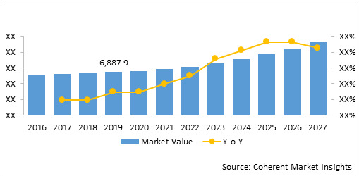
With products, services and applications, valued US$ 6,887.9 Mn in 2019, the global microscopy devices market is forecast to reach a value of US$ 17,130.4 Mn by 2027 at a CAGR of 12.1% from 2020 to 2027.
The global microscopy devices market, manufacturing and service is estimated to reach US$ 17,130.4 Mn in terms of valuation, as increasing prevalence of chronic disorders, increasing research & development, and adoption of expansion strategies from major companies are the major factors behind the driving force of the exponential growth in the microscopy devices market.
Request for Sample PDF Copy: https://www.coherentmarketinsights.com/insight/request-sample/3924
Description:
Optical magnifying lens, electron magnifying instruments, and examining test magnifying lens are a portion of the sorts of microscopy gadgets utilized in the social insurance part. Optical magnifying lens are additionally divided into altered magnifying lens, stereomicroscopes, stage differentiate magnifying lens, confocal examining magnifying instruments, close to handle filtering magnifying instruments and other optical magnifying instruments.
Statistics:
The global microscopy devices market is estimated to account for US$ 17,130.4 Mn in terms of value by the end of 2027.
Global Microscopy Devices Market: Drivers
Endorsement and dispatch of new gadgets is relied upon to drive development of the worldwide microscopy gadgets showcase over the figure time frame. For example, in May 2018, Tomey USA got the U.S. Food and Drug Administration freedom of its EM-4000 Specular Microscope, which highlights Core strategy to tally cells and can yield information and pictures to an EHR server or independent PC.
In addition, expanding pervasiveness of visual issues is likewise expected to help in development of the market. For example, as indicated by National Eye Institute's projections, the quantity of individuals in the U.S. with waterfall is required to arrive at 50 million of every 2050.
Statistics:
Asia Pacific held dominant position in the global microscopy devices market in 2019, accounting for 33.0% share in terms of value, followed by North America and Europe, respectively
Global Microscopy Devices Market: Restraints
Light microscopes are complex and house numerous fine-tuned lenses with tightly controlled dimensions. These microscopes require special and complex sample preparation techniques or the samples either get destroyed or structurally altered when viewed. Such scenario is expected to hinder growth of the market.
Moreover, high cost of microscopy devices is also expected to limit the market growth. For instance, Helios NanoLab Dual Beam SEM from FEI Company sells at US$ 2.2 million, Libra 200 TEM from Zeiss is priced at US$ 2.5 million, and Titan G2 80-200 scanning transmission electron microscope (S/TEM) at US$ 12.8 million.
Global Microscopy Devices Market: Opportunities
Increasing geriatric population is expected to offer lucrative growth opportunities for players in the global microscopy devices market. For instance, according to the U.S. Census Bureau, the U.S. geriatric population is expected to reach 77 million by 2034.
Moreover, activities to increase the number of eye clinics is also expected to aid in growth of the market. For instance, in March 2019, Covenant Surgical Partners partnered with U.S.-based De La Peña Eye Clinic to expand its eye surgery centers.
Statistics:
The global microscopy devices market was valued at US$ 6,887.9 Mn in 2019 and is forecast to reach a value of US$ 17,130.4 Mn by 2027 at a CAGR of 12.1% between 2020 and 2027.
Market Trends/Key Takeaways
Significant players in the market are additionally centered around receiving M&A procedures to extend their item portfolio. For example, in April 2018, Topcon Corporation declared that Topcon Healthcare Solutions, an auxiliary in the U.S., gained all the remarkable portions of KIDE Clinical Systems Oy, a supplier of optical and ophthalmology cloud arrangements.
The covid-19 pandemic has driven makers to discharge rules with respect to cleaning their items. For example, in April 2020, NIDEK Co., Ltd. discharged rules expressing that parts reached with the patient and lodging for NIDEK items can be cleaned up with a fabric hosed with liquor.
Global Microscopy Devices Market: Competitive Landscape
Significant players working in the worldwide microscopy gadgets advertise incorporate, Cameca SAS, Hitachi High-Technologies Corporation, Thermo Fisher Scientific, FEI Company, Olympus Corporation, Nikon Corporation, Carl Zeiss AG, Bruker Corporation, Leica Microsystems, NT-MDT Company, Tomey USA, NIDEK Co., Ltd., Topcon Corporation, and Danish Micro Engineering A/S.
Global Microscopy Devices Market: Key Developments
Significant players in the market are centered around embracing cooperation and organization techniques to improve their piece of the overall industry. For example, in December 2019, Leica Microsystems teamed up with the European Molecular Biology Laboratory for the improvement of new imaging advancements.
Figure 1: Global Microscopy Devices Market Share (%) Value, By Region, 2019
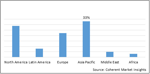
Figure 2: Global Microscopy Devices Market Value (US$ Mn), 2016 – 2027
Buy this Research Report: https://www.coherentmarketinsights.com/insight/buy-now/3924
About Us:
Coherent Market Insights is a global market intelligence and consulting organization focused on assisting our plethora of clients achieve transformational growth by helping them make critical business decisions. We are headquartered in India, having office at global financial capital in the U.S. Our client base includes players from across all business verticals in over 150 countries worldwide. We do offer wide range of services such as Industry analysis, Consulting services, Market Intelligence, Customized research services and much more. We have expertise in many fields such as healthcare, chemicals and materials, Automation, semiconductors, electronics, energy, food and beverage, packaging and many more. Visit our website to know more.
Contact Us:
Mr. Shah
Coherent Market Insights
1001 4th Ave.
#3200
Seattle, WA 98154
Tel: +1-206-701-6702
Email: [email protected]
1 note
·
View note
Photo


ION BEAMS AND ATOM SMASHERS: SECRETS OF MOON ROCKS On July 20, 1969, as Apollo astronaut Neil Armstrong climbed down the ladder from the “Eagle” lunar landing module, he found himself surrounded by a sea of grey -- an expanse of powdery dust no human had ever seen in person. The iconic print made by his left boot marked but the first step on a long journey of discoveries about the Moon and our own world -- both of which hold secrets that scientists are only beginning to uncover. Fifty years after the Apollo astronauts collected samples of Moon rocks and dust during their forays across the lunar landscape, there are still mysteries to be solved, and one University of Arizona scientist is looking for answers. Jessica Barnes, an incoming assistant professor in the UA’s Lunar and Planetary Laboratory, was recently selected by NASA to receive access to preciously unopened Moon rock samples. Under NASA’s Apollo Next Generation Sample Analysis, or ANGSA, program, Barnes will be granted access to Apollo 17 sample 71036, which contains almost four ounces of rock. Several samples from that mission were initially processed under nominal laboratory conditions, protected from air exposure by a nitrogen cabinet at room temperature, and placed into cold storage within one month of return. “When these samples were brought back, the curators had the foresight to say, ‘In this moment, we don’t have all the methods to answer all the questions these samples could help us answer,’ and so they locked some away for future study,” Barnes says. “They realized that future technologies would allow us to do things that would have been impossible at the time, and that people would come up with new questions. It’s really exciting because we’re at that point in time now.” Barnes is on a quest to find out where water came from in the early solar system and how it has evolved over time. Previous research, including some of her own work, suggests that certain space rocks known as carbonaceous chondrites brought water with them when they impacted Earth and Mars, and potentially some of the larger asteroids. It is no coincidence that Bennu, the target asteroid of the UA-led OSIRIS-REx sample return mission, is a carbonaceous chondrite. “To understand where water in the solar system came from, and particularly how it ended up on Earth, Mars, and in the asteroid belt, we have to consider the Moon,” says Barnes, whose current research focuses on tracing water meteorites, including some of Martian origin, and Moon samples collected during Apollo 11, 14, and 17. “Understanding how life on Earth began is intimately tied to the story of how water arrived here. Lunar samples are critical pieces in this puzzle because unlike Earth, where the oldest rocks have largely been erased by plate tectonics, the Moon’s ancient rock record is still intact.” About 4.6 billion years ago, when a swirling nebula of gas and dust began collapsing into a disk that would give rise to our solar system, the rocky planets and the carbonaceous chondrites were developing in different places and at different times, Barnes explains, which poses a problem for the scenario involving early asteroids as harbingers of water. “It was only 10 years ago that water was discovered on the Moon, not only on the surface, but also inside minerals,” Barnes says. “In science, that is a pretty short timescale, and we don’t have it all figured out yet. How much water is there? Did it come from the Earth during the great impact that we think created the Moon, or was it given to the Moon later? Is it distributed uniformly or in patches within the Moon’s mantle?” To find answers to such questions, Barnes, who wasn’t even born when the Apollo astronauts crisscrossed the lunar surface on foot and with their rovers, is using technology that wasn’t invented until the early 2000s. “When you first receive your sample, you don’t know what you are looking at, so you start with a visual analysis,” Tom Zega says, pointing to a simple dissecting microscope, like the ones used in introductory science labs. Zega is an associate professor of planetary sciences, and materials science and engineering, and co-investigator on the ANGSA project. He also is director of the Kuiper Materials Imaging and Characterization Facility at the LPL, a state-of-the-art facility designed with one goal: extract as much information as possible from samples, both terrestrial and extraterrestrial. Studying a piece of Moon rock under an optical microscope is only the first step in a series of analytical techniques UA researchers have at their disposal. At the end is a 12-foot-tall transmission electron microscope, or TEM. Funded by the National Science Foundation and NASA, its serial number is “1” because it is the first of its kind in the world with this exact configuration. Its 200,000-volt electron beam can probe matter down to 78 picometers, scales too small for the human brain to comprehend. “If you want to know what an atom from the birth of our solar system looks like, I can show you,” Zega says. To get a sample to where it gives up that much detail of its origin and history, however, requires a suite of complex instruments and expertise that no single discipline can provide. “Today, all the interesting science happens at the intersection of various fields,” Zega added. “In my group, we have cosmochemists, quantum chemists, astrophysicists and astrodynamics, among others. This work requires a unique mix of knowledge and skills. Take the TEM, for example: it’s a quantum-mechanical tool, so you have to be an expert in physics, materials science and chemistry, all at the same time.” Another instrument, called an electron microprobe, allows researchers to discover certain properties of a sample by scanning it with an electron beam. As it does, a spatial image of the sample emerges, in this case revealing an abstract, speckled landscape of light and dark areas that cosmochemists can read like a map. “Heavier elements appear brighter, and lighter elements appear darker,” Zega says. “So this tells us, for example, where and how much iron there is compared to oxygen in a lunar sample.” When Barnes moves to the UA this fall, after wrapping up her current research at NASA’s Johnson Space Center, she hopes to be able to expand the capacities of the Kuiper Materials Imaging and Characterization Facility with a next-generation NanoSIMS instrument, which stands for nanoscale secondary ion mass spectrometry. The beauty of this technology, she says, lies in its ability to analyze isotopes, essentially different “varieties” of chemical elements, at very small scales -- less than one-fiftieth the width of a human hair. Measuring the composition of different volatile elements such as hydrogen and chlorine in the rock tells the researcher something about the chemical make-up of the magma from which the rock crystallized and how its chemistry evolved over time. “These data allow us to understand the chemistry of the Moon’s interior,” Barnes says. “Ultimately we are able to say something about how the Moon evolved and where its water came from.” The possibilities don’t end here. To a curator during the Apollo days, a focused ion-beam scanning electron microscope, or FIB-SEM, would have sounded like utter science fiction: By smashing the bonds between atoms inside the sample with a beam of heavy gallium ions, the instrument works essentially like a nano scale excavator, Zega explains. “Except that compared to other FIBs, which act like shovels, this one is a scalpel,” he says. FIB-SEM allows scientists to cut out tiny pieces from a sample with high precision and analyze only those pieces. This technique recently enabled Zega’s team to discover a grain of dust forged in the death throes of a star long before our solar system was born. “What we want to know from our samples is, how well do they conform to how we think the solar system formed based on astrophysical models?” Zega says. The same applies to the origin of the Moon, Barnes says. “It’s not just analytical instruments that have improved. In the last 10 years, major advancements in impact simulations and numerical modeling have allowed the community to simulate the speed, size and number of the bodies that might have been involved in creating the Earth-Moon system.” Analyzing samples from extraterrestrial bodies goes beyond the origins of the Earth and the Moon, of course. They are critical pieces in the puzzle because they allow scientists to test hypotheses about formation processes in the solar system based on simulations and models. “We have had lunar samples here for decades,” says Timothy Swindle, director of the LPL. “Our faculty have been studying the composition of the Moon for a long time, and what’s so special about these samples is that they were valuable 50 years ago, and they will be valuable 50 years from now.” “Being able to study these previously unopened samples is like a whole new lunar sample return mission,” Barnes says of the value of studying 50-year-old Apollo samples. “Not only do we get to be a part of the history of opening these samples, but we also will be using this opportunity to study how curation practices, such as ambient versus cold storage, affect our ability to measure a lunar water signature. “It’s exciting because this has never been done before.” TOP IMAGE....A NanoSIMS isotope ratio image showing water-bearing minerals (colors) in a sea of water-poor glass (black) in Apollo sample 10049. These were the last phases to crystallize from the lava as it cooled on the surface of the Moon. The scale bar on the lower left measures about one-fiftieth the width of a human hair. (Image: Jessica Barnes) LOWER IMAGE....Apollo 17 astronaut Harrison “Jack” Schmitt stands next to a steep-walled crater named Shorty on Dec. 13, 1972. The UA's Jessica Barnes is among the scientists selected by NASA to be granted access to previously unopened samples, including some collected during NASA's last manned mission to the moon. (Photo: NASA)
4 notes
·
View notes
Text
Failure Analysis Equipment Market Research Report - Global Forecast to 2030
Failure Analysis Market Highlights
Acknowledging the prominence and traction, the market is garnering currently Market Research Future (MRFR) in its recently published study report asserts that the global Failure Analysis Market will garner exponential accruals by 2023, registering approximately 8% CAGR throughout the review period (2017-2023).
Failure Analysis can be defined as the process used for logical and systematic investigation of equipment or machine or its documentation to detect and analyse the causes, probabilities, and consequences of actual or potential failure. The failure analysis market is growing pervasively mainly due to the proliferation of hand-held electronic devices, creating a huge demand for semi-conductors. The rising awareness among people regarding the quality of product or solutions escalates the market growth on the global platform.
Key Players:
Fervent players driving the market for the failure analysis include FEI Company (U.S.), Carl Zeiss SMT GmbH (Germany), JEOL Ltd. (Japan), Tescan (U.S.), Hitachi High- Technologies (Japan), EAG Inc. (Luxembourg), Raytheon Company (U.S.), and Intertek Group plc (United Kingdom).
Get Free Sample Copy at: https://www.marketresearchfuture.com/sample_request/6092
Moreover, factors such as the advantageous features of failure analysis like scalability and cost optimization along with the proliferation of connected devices allow market to grow at large, fetching many benefits to industries.
Furthermore, factors propelling the market growth include the increasing industrialization and the improving economic conditions worldwide.
On the other hand, failure analysis being in its embryonic stage still presents the challenges such as lack of universally accepted testing standards while, the initial investment required for the implementation of failure analysis acts as a headwind that obstructs the market growth.
Global Failure Analysis Market - Segments
The analysis has been segmented into five key dynamics for the better scope: -
By Equipment : Scanning electron microscope (SEM), Transmission Electron Microscopy (TEM), Focused Ion Beam (FIB), and Dual Beam FIB among others.
By Technology : SIMS, EDX, CMP, FIB, BIM and RIE.
By Testing : Material Testing, Non-destructive Testing (NDT), and Physical Testing.
By Application : Material Science, Bio Science, Industrial, and Electronics.
By Region : North America, Europe, APAC and the Rest-of-the-World.
Global Failure Analysis Market - Regional Analysis
Globally, the North American region accounts for the leading market for the failure analysis. Advancements in technologies and market proliferation of portable electronics devices are expected to support the market growth to retain its dominance over the global failure analysis market throughout the forecast period.
Presence of well-established infrastructures along with the presence of well-established key players in the region acts as a tailwind that pushes up the growth of the regional market, allowing a favorable environment for technological developments. The market is estimated to witness a higher adoption of failure analysis tools owing to the government’s efforts to push the markets for material testing.
The Asia Pacific region is projected to grow at the fastest rate during the forecast period, emerging as a promising market for failure analytics. Factors such as the presence of major semiconductor industries and the rising adoption of failure analysis solutions to fight out the risks such as chemical explosion drive the market growth in the region.
Furthermore, the augmenting demand for deployment of failure analysis technologies alongside the massive demand for the advanced analytics solutions help increase the market size, facilitating enterprises to comprehend business scenarios.
Failure Analysis Market – Competitive Analysis
Highly competitive by nature, the global failure analysis market appears to be fragmented due to the presence of many players. Key strategies traced from the analysis of recent developments of the market players include agreement & partnership, acquisition expansion, and product launch. These key players strive to deliver comprehensive testing solutions with adept technology and features. Growth in terms of product innovations and technologies in the market are also expected to create strong investment opportunities for the global players.
Get Complete Report Details at: https://www.marketresearchfuture.com/reports/failure-analysis-market-6092
About Market Research Future:
At Market Research Future (MRFR), we enable our customers to unravel the complexity of various industries through our Cooked Research Report (CRR), Half-Cooked Research Reports (HCRR), Raw Research Reports (3R), Continuous-Feed Research (CFR), and Market Research & Consulting Services.
MRFR team have supreme objective to provide the optimum quality market research and intelligence services to our clients. Our market research studies by products, services, technologies, applications, end users, and market players for global, regional, and country level market segments, enable our clients to see more, know more, and do more, which help to answer all their most important questions.
Contact:
Market Research Future (Part of Wantstats Research and Media Private Limited)
99 Hudson Street, 5Th Floor
New York, NY 10013
United States of America
+1 628 258 0071 (US)
+44 2035 002 764 (UK)
Email: [email protected]
Website: https://www.marketresearchfuture.com
0 notes
Photo

Machine learning technique speeds up crystal structure determination
Nanoengineers at the University of California San Diego have developed a computer-based method that could make it less labor-intensive to determine the crystal structures of various materials and molecules, including alloys, proteins and pharmaceuticals. The method uses a machine learning algorithm, similar to the type used in facial recognition and self-driving cars, to independently analyze electron diffraction patterns, and do so with at least 95% accuracy.
The work is published in the Jan. 31 issue of Science.
A team led by UC San Diego nanoengineering professor Kenneth Vecchio and his Ph.D. student Kevin Kaufmann, who is the first author of the paper, developed the new approach. Their method involves using a scanning electron microscope (SEM) to collect electron backscatter diffraction (EBSD) patterns. Compared to other electron diffraction techniques, such as those in transmission electron microscopy (TEM), SEM-based EBSD can be performed on large samples and analyzed at multiple length scales. This provides local sub-micron information mapped to centimeter scales. For example, a modern EBSD system enables determination of fine-scale grain structures, crystal orientations, relative residual stress or strain, and other information in a single scan of the sample.
Read more.
#Materials Science#Science#Crystal structure#Computational materials science#Materials Characterization#UC San Diego#Electron backscatter diffraction#EBSD
56 notes
·
View notes
Text
Science and Chemistry Classes
New method measures nanoscale material response at high magnification
by University of Illinois at Urbana-Champaign
The safety glass used in the windshields of limousines and military vehicles needs to be hard, strong and shatter-proof, but also thin—both for visibility and to reduce its weight, a particularly important feature for aerospace vehicles. The use of a promising new transparent ceramic spinel that could replace traditional layered safety glass was the motivation for recent research at the University of Illinois Urbana-Champaign that resulted in a new method to measure changes that occur in materials, such as glasses, at the nanoscale.
"We used a transmission electron microscope, which has been used extensively for imaging materials at the molecular, granular or sub-granular level, to help us understand how these materials behave, because in the electron microscope the electron beam wavelength can probe smaller distances than the visible light microscope," said John Lambros, professor in the Department of Aerospace Engineering and director of the Advanced Materials Testing and Evaluation Laboratory at Illinois.
"Beyond imaging, however, we wanted to turn the electron microscope into a full-field metrology measurement instrument. Measurements in the electron microscope have been made before, but only at individual points through particle tracking. We added digital image correlation capabilities which we extended for use in this very high-magnification, high-resolution microscope instrument."
Lambros explained that electron microscopes bring unique challenges for the digital, image correlation metrology that had to be overcome.
"Because instead of a light beam, you have an electron beam illuminating the sample, the transmission electron microscope is a much harsher environment. It's very difficult to operate and it's all done in vacuum," he said. "Imaging is much more difficult and the samples are very small scale."
The researchers first ion-milled a bend-beam from a bulk piece of silicon dioxide, a type of glass, in the Materials Research Laboratory's focused ion beam facility. In a vacuum deposition chamber, a thin film of gold is deposited on the beam. Then, the sample is heated and the continuous film breaks up into little islands, which provide sufficient contrast to be visible on the silica sample in the electron microscope.
"With a scanning electron microscope, the images are of the sample surface because the electron beam bounces off the surface," Lambros said. "But in the transmission electron microscope the electron beam goes through the sample, which must be very thin, and the response is averaged through the thickness. Digital Image Correlation in the SEM has been used for a long time because it's so much easier to get images there. This has not been done using the TEM, which has much higher magnification capabilities, and this is why we wanted to extend the digital image correlation method to the TEM."
The researchers took images over time, up to 300 seconds, while the sample was subjected to a bending load, and compared image to image to measure how the gold particles deposited on the surface move.
"Digital image correlation takes a series of images of the gold dots as the loading is progressing. And by comparing one image to the next you can map what is happening—and not just around the edges, but internal features inside the sample," Lambros said. "So, in this project, we used particle tracking as a check, or control, and then demonstrated the highly comparable results using digital image correlation in the TEM."
Lambros explained that with particle tracking, there are typically fewer particles tracked which means fewer measurement points. And compared to DIC, the particle must move larger amounts for us to be able to see movement in an image.
"This study is about developing the digital image correlation method in the transmission electron microscope. Now that we have confirmation that the method works, we can replicate it and use it to study the nanoscale behavior of the spinel material, which was our initial interest," Lambros said.
He said they have started the spinel studies by putting the gold particles to create a pattern on sample of spinel but have not tried it in the transmission electron microscope yet.
"The patterning works on spinel, but there will be other issues with spinel because it's crystalline and crystals behave very differently in the TEM than amorphous glass," Lambros said. "In experimental mechanics one of our biggest constraints is that we mainly look at what's happening on the surface. We try to deduce from that what's happening inside the material and that's a difficult task. This method is really ground-breaking because now we'll be able to image materials in a new way and at a very high magnification."
The study, "Full-field deformation measurements in the transmission electron microscope using digital image correlation and particle tracking," written by AE Ph.D. student Yiguang Zhang, Lin Feng, Shen Dillon, and John Lambros, is published in Materials Characterization.
0 notes
Link
Global Electron Microscope Market
0 notes
Text
Microstructural analysis empowers researchers to design advanced materials, enhance quality control
Metallurgy is a fascinating field that deals with the study of metals and their alloys, focusing on their structure, properties, and performance. One of the fundamental aspects of metallurgical research is microstructural analysis. This technique involves the examination of small-scale structures within metals and alloys, providing valuable insights into their behavior and characteristics. In this article, we will delve into various techniques used for microstructural analysis in metallurgy and explore their significant applications in the industry.

Metnmat Research and Innovation
Table of Contents
Introduction
Understanding Microstructural Analysis
Sample Preparation Techniques
Optical Microscopy
Scanning Electron Microscopy (SEM)
X-ray Diffraction (XRD)
Transmission Electron Microscopy (TEM)
Ultrasonic Testing
Image Analysis and Digital Microscopy
Applications of Microstructural Analysis in Metallurgy Future Trends in Microstructural Analysis
Conclusion
FAQs
Introduction
Metals and alloys are integral to various industries, from aerospace and automotive to electronics and construction. To ensure their optimal performance and reliability, it is essential to understand their microstructure, which directly influences their mechanical, thermal, and electrical properties.
Understanding Microstructural Analysis
Microstructural analysis is a vital tool in the field of metallurgy, as it allows researchers to observe and understand the internal structure of metals and alloys at a microscopic level. By examining the arrangement of grains, phases, inclusions, and defects within the material, metallurgists can gain valuable information about its properties and performance. This knowledge is crucial for various applications, from material design and manufacturing to failure analysis and quality control.
The first step in microstructural analysis is sample preparation. Proper sample preparation is essential to obtain accurate and reliable results. It involves cutting the metal sample into manageable sections and mounting it on a substrate to facilitate handling during subsequent preparation steps. Grinding and polishing are then performed to achieve a smooth and flat surface, ready for microscopic examination. Finally, etching is conducted to reveal the microstructure's features, making them more visible under a microscope.
Sample Preparation Techniques
Before conducting microstructural analysis, proper sample preparation is crucial to obtain accurate and reliable results. The following techniques are commonly used:
Cutting and Mounting
Samples are carefully sectioned and mounted on a substrate to facilitate handling during subsequent preparation steps.
Grinding and Polishing
Grinding and polishing are performed to achieve a smooth and flat surface, ready for microscopic examination.
Etching
Etching is a chemical process used to reveal the microstructure's features, making them more visible under a microscope.
Optical Microscopy
Optical microscopy is one of the most widely used techniques for microstructural analysis in metallurgy. It involves the use of visible light to examine the metal sample's microstructure. With a wide range of magnifications available, optical microscopy is suitable for routine examination of metal structures.
Stereomicroscopy is a variation of optical microscopy that provides a 3D view of the sample's surface. This is particularly useful for studying surface defects and coatings. Polarized light microscopy (PLM) is employed to study birefringent materials, providing information about crystallographic orientations. Darkfield microscopy, on the other hand, enhances the contrast of transparent phases, helping to identify small particles or precipitates.
Light Microscopy
Light microscopy is employed for routine examination of metal structures with a wide range of magnifications.
Stereomicroscopy
Stereomicroscopy provides a 3D view of the sample's surface, aiding in the study of surface defects and coatings.
Polarized Light Microscopy (PLM)
PLM is utilized to study birefringent materials, revealing information about crystallographic orientations.
Darkfield Microscopy
Darkfield microscopy enhances the contrast of transparent phases, useful for identifying small particles or precipitates.
Scanning Electron Microscopy (SEM)
SEM allows for high-resolution imaging and 3D visualization of a sample's surface using electrons.
Scanning Electron Microscopy (SEM) is an advanced technique used for high-resolution imaging and 3D visualization of a metal sample's surface. Instead of using light, SEM utilizes a focused beam of electrons to interact with the sample. As the electrons interact with the surface, various signals, such as secondary electrons and backscattered electrons, are generated, which are then detected to form an image.
SEM is particularly valuable for investigating surface topography and identifying surface features at a nanoscale level. The high magnification and resolution capabilities of SEM make it an essential tool for researchers and engineers in metallurgy.
"Microstructural analysis empowers researchers to design advanced materials, enhance quality control, and drive innovation across diverse industries."
X-ray Diffraction (XRD)
X-ray Diffraction (XRD) is another powerful technique used for microstructural analysis in metallurgy. XRD is based on the principle of X-ray scattering by the crystal lattice of a material. When X-rays interact with the crystal lattice, they are diffracted in specific directions, producing a diffraction pattern. This pattern is characteristic of the crystal structure and phases present in the material.
By analyzing the diffraction pattern, researchers can identify the crystal structures and phases in the metal sample, providing crucial information about its composition and microstructure. XRD is especially useful for analyzing powdered samples and identifying unknown materials.
Transmission Electron Microscopy (TEM)
TEM is an advanced technique that enables the examination of the internal microstructure at the nanoscale.
Transmission Electron Microscopy (TEM) is an advanced technique that enables researchers to examine the internal microstructure of metals and alloys at an incredibly high resolution. TEM works by transmitting a focused beam of electrons through a thin sample, which is then magnified to form an image on a fluorescent screen or a digital detector.
TEM allows for the visualization of individual grains, dislocations, and other fine microstructural features at the nanoscale level. This level of detail is essential for understanding the behavior of materials, especially in high-tech applications and research.
Ultrasonic Testing
Ultrasonic testing measures the ultrasonic waves' velocity through a material, helping to detect defects and assess material integrity.
Ultrasonic Testing (UT) is a non-destructive testing technique used to assess the integrity of a material or detect defects within it. In ultrasonic testing, high-frequency sound waves, usually in the range of 0.5 to 10 MHz, are introduced into the material. These sound waves travel through the material until they encounter a boundary or defect, where they are reflected back to a receiver.
By analyzing the time it takes for the sound waves to return and the amplitude of the returning waves, researchers can determine the presence and location of defects, such as cracks or voids. UT is commonly used for quality control in manufacturing and inspection of welded joints.
Image Analysis and Digital Microscopy
Image analysis software is used to quantify and characterize microstructural features, providing valuable data for research and development.
Digital microscopy, in combination with image analysis, enables researchers to perform complex measurements and calculations on the microstructural features of metals and alloys. This data is used to evaluate the effects of different processing techniques, assess the material's properties, and optimize the performance of metal components.
"From optical microscopy to transmission electron microscopy, explore the cutting-edge techniques that reveal the intricate world of metal microstructures."
Applications of Microstructural Analysis in Metallurgy
Microstructural analysis plays a pivotal role in various applications within the field of metallurgy:
microstructural analysis plays a pivotal role in various applications within the field of metallurgy. The knowledge gained from these analyses informs critical decisions in material design, manufacturing processes, and performance evaluation.
One of the primary applications of microstructural analysis is quality control in manufacturing. By examining the microstructure of metal samples, manufacturers can ensure the consistency and quality of their products. Any variations or defects in the microstructure can be detected and addressed early in the production process, preventing potential issues down the line.
microstructural analysis is essential in evaluating heat treatment processes. Heat treatment is commonly used to alter the microstructure of metals, improving their mechanical properties. By analyzing the microstructure after heat treatment, researchers can optimize the process to achieve the desired material properties.
Quality Control in Manufacturing
By analyzing the microstructure, manufacturers can ensure the consistency and quality of their products.
Failure Analysis
In cases of component failure, microstructural analysis helps identify the root cause and prevent future occurrences.
Material Characterization
The microstructural analysis aids in understanding the material's properties and behavior under different conditions.
Welding and Joining
Evaluation of microstructures in welded or joined materials ensures structural integrity and performance.
Corrosion Studies
Studying the microstructure helps in understanding corrosion mechanisms and selecting corrosion-resistant materials.
Heat Treatment Evaluation
The microstructural analysis is vital for optimizing heat treatment processes and achieving desired material properties.
Future Trends in Microstructural Analysis
The field of microstructural analysis continues to evolve, with ongoing advancements in imaging techniques and data analysis methods.
Another exciting trend is the development of in-situ microstructural analysis methods. In-situ techniques allow researchers to study the evolution of microstructures under specific conditions, such as temperature or mechanical stress. These methods provide valuable insights into how microstructures change over time and can help optimize processes or predict material behavior under different environmental conditions.
Advancements in data analysis and machine learning also hold great promise for microstructural analysis. With the increasing volume of data generated by various microscopy techniques, sophisticated data analysis tools are essential for extracting meaningful information. Machine learning algorithms can identify patterns and correlations within large datasets, facilitating more accurate material property predictions and improved material design.
"Unlocking the hidden secrets within metals and alloys through microstructural analysis is the key to optimizing their performance and reliability."
Conclusion
Microstructural analysis in metallurgy is a critical discipline that provides valuable insights into the properties and behavior of metals and alloys. By employing various advanced techniques, researchers and engineers can make informed decisions in material design, manufacturing, and performance evaluation.
As technology continues to advance, we can expect further innovations in microstructural analysis methods, enabling more detailed and precise examination of materials. These developments will undoubtedly lead to the creation of novel materials with enhanced properties, contributing to the improvement of various industries and applications.
The future of microstructural analysis is promising, and ongoing research in this field will undoubtedly shape the way we understand and utilize metals and alloys in the years to come.
FAQs
Q. What is the significance of microstructural analysis in metallurgy?
Microstructural analysis helps in understanding the relationships between a material's structure and its properties, enabling better material design and selection for specific applications.
Q. Which technique is best suited for studying grain boundaries in metals?
Transmission Electron Microscopy (TEM) is exceptionally well-suited for studying grain boundaries at the nanoscale.
Q. Can microstructural analysis identify the presence of impurities?
Yes, microstructural analysis can reveal the presence of impurities and their distribution within the material.
Q. How does microstructural analysis contribute to alloy development?
The microstructural analysis allows researchers to assess the microstructure-property relationships, aiding in the development of new and improved alloys.
Q. Is microstructural analysis applicable to non-metallic materials?
Yes, microstructural analysis techniques can be adapted to study the microstructures of non-metallic materials, including ceramics and polymers.
Reach Us Now.
#Metallurgy#Microstructural Analysis#Techniques#Materials#Metals#Alloys#Material Characterization#Manufacturing#Research
0 notes
Last Seen Blogs

potter-solomons
to observe & reflect

leeknowpegger
c&bt

reykjaviksessions
@neverlandmylove

thedimplesonmythighs
The Dimples On My Thighs

thickenmyblood
thicken my blood