#Chemical mechanical planarization
Text
Chemical Mechanical Planarization Market to Exceed USD 12 Billion by 2031
The global Chemical Mechanical Planarization (CMP) market is projected to witness substantial growth from 2023 to 2031, driven by the increasing demand for advanced semiconductor manufacturing processes, the proliferation of electronic devices, and the expansion of the automotive and aerospace industries. CMP is a critical process used in semiconductor fabrication, optics, and other precision manufacturing industries to achieve ultra-flat and smooth surfaces.
The chemical mechanical planarization market was worth US$ 5.6 billion in 2021, and the market is projected to reach US$ 12 billion by 2031. Chemical mechanical planarization sales are projected to increase at a CAGR of 7.9% until 2031.
A critical part of manufacturing MEMS devices is the manufacturing process of the CMP, which is used widely across several industries, including consumer electronics, automotive, healthcare, and industrial applications. A major driving force behind the growth of the CMP market is the development of MEMS technologies.
Get Access to Sample Research Report with Latest Industry Insights @ https://www.transparencymarketresearch.com/sample/sample.php?flag=S&rep_id=19007
Market Segmentation:
The CMP market can be segmented based on several factors including service type, sourcing type, application, industry vertical, and region. Understanding these segments facilitates a detailed analysis of specific market trends and dynamics.
By Service Type: Equipment, Consumables (Abrasive, Pad, Slurry)
By Sourcing Type: In-house, Outsourced
By Application: Semiconductor Manufacturing, Optics, Data Storage, MEMS, Others
By Industry Vertical: Electronics, Automotive, Aerospace, Healthcare, Others
By Region: North America, Europe, Asia-Pacific, Latin America, Middle East & Africa
Regional Analysis:
North America: Leading market due to the presence of key semiconductor manufacturers, technological advancements, and increasing investments in R&D.
Europe: Significant market share attributed to the growing automotive and aerospace industries and the increasing demand for high-performance electronic devices.
Asia-Pacific: An emerging market with rapid industrialization, extensive semiconductor manufacturing activities, and significant investments in infrastructure development.
Latin America: Growing adoption of CMP technology in electronics manufacturing and increasing investments in semiconductor fabrication facilities.
Middle East & Africa: Rising demand for advanced electronics and semiconductor components driving market growth in the region.
Market Drivers and Challenges:
Drivers:
Increasing demand for high-performance electronic devices and advanced optics.
Continuous advancements in semiconductor manufacturing processes.
Growing applications of CMP in emerging technologies such as 3D integration and MEMS.
Challenges:
Technological complexities associated with achieving ultra-flat and smooth surfaces.
Environmental and safety concerns related to chemical usage in CMP processes.
Intense competition from alternative surface finishing technologies.
Market Trends:
Integration of CMP with advanced process control technologies for enhanced precision and efficiency.
Development of next-generation CMP slurries and pads for improved material removal rates and surface quality.
Adoption of CMP in novel applications such as compound semiconductor manufacturing and advanced packaging.
Future Outlook:
The future outlook for the CMP market appears promising, driven by the increasing demand for high-performance electronic devices, advancements in semiconductor manufacturing processes, and the growing adoption of CMP in emerging applications. Market players are expected to leverage technological innovations and strategic partnerships to capitalize on evolving market trends and gain a competitive edge.
Key Market Study Points:
Analysis of market dynamics including drivers, challenges, and opportunities.
Assessment of market segmentation and regional trends.
Evaluation of competitive landscape and key market players.
Examination of recent developments and emerging trends shaping the market.
Competitive Landscape:
The CMP market is characterized by intense competition among key players striving to enhance their market presence through product innovation, strategic partnerships, and expansion strategies. Major players in the market include:
Applied Materials, Inc.
Ebara Corporation
Cabot Microelectronics Corporation
Entegris, Inc.
Fujimi Incorporated
Recent Developments:
Launch of advanced CMP equipment and consumables catering to specific customer requirements.
Strategic collaborations with semiconductor manufacturers and research institutions to drive innovation.
Investments in R&D to develop next-generation CMP technologies and materials.
Place an Order Copy of the Chemical Mechanical Planarization Market Report at: https://www.transparencymarketresearch.com/checkout.php?rep_id=19007<ype=S
About Transparency Market Research
Transparency Market Research, a global market research company registered in Wilmington, Delaware, United States, provides custom research and consulting services. Our exclusive blend of quantitative forecasting and trends analysis provides forward-looking insights for thousands of decision-makers. Our experienced team of Analysts, Researchers, and Consultants use proprietary data sources and various tools & techniques to gather and analyze information.
Our data repository is continuously updated and revised by a team of research experts so that it always reflects the latest trends and information. With a broad research and analysis capability, Transparency Market Research employs rigorous primary and secondary research techniques in developing distinctive data sets and research material for business reports.
Contact:
Transparency Market Research Inc.
CORPORATE HEADQUARTER DOWNTOWN,
1000 N. West Street,
Suite 1200, Wilmington, Delaware 19801 USA
Tel: +1-518-618-1030
USA – Canada Toll Free: 866-552-3453
Website: https://www.transparencymarketresearch.com
0 notes
Video
Chemical mechanical planarization (CMP) is one of the crucial steps used multiple times during the manufacture of semiconductors. This process is used at every layer of wafer for removing excess material and for creating a smooth surface with the help of a liquid known as CMP slurry.
Read more- https://cmiblogdailydose.blogspot.com/2022/07/cmp-slurry-is-abrasive-powder-used-in.html
#Chemical mechanical planarization#CMP#Advanced materials#Coherent Market Insights#semiconductors#manufacturing
0 notes
Note
death to haas my undying loyalty lies with fanutrol integrated machines
My work machines come from a Shenzhen company called JiuTu and they use the YouTube logo lmao

#theyre 'chemical mechanical planarization' machines#they hold phones sealed in molds against spinning carpets that polish the screen using an abrasive#im 'in charge' of all the machine line and drainage and engineering the workflow for the polishing area#i also just got a new dry polisher actually and im waiting for double the pneumatic machines!#i also have a tank meant for holding and mixing milk for the fluid#also some auto glue machines#all from jiutu lol but i plan on domestic repair sources
4 notes
·
View notes
Text
Polymer CMP Pads, Global Market Size Forecast, Top 10 Players Rank and Market Share
Polymer CMP Pads Market Summary
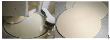
Chemical mechanical polishing/planarization (CMP) is a process that removes materials by a combination of chemical and mechanical (or abrasive) actions to achieve highly smooth and planar material surfaces. Chemical-mechanical polishing (CMP) is often associated with chemical-mechanical planarization which is a polishing process assisted by chemical reactions to remove surface materials. CMP is a standard manufacturing process practiced at the semiconductor industry to fabricate integrated circuits and memory disks. When the purpose is to remove surface materials, it is referred to as chemical-mechanical polishing. However, when the purpose is to flatten a surface, it is referred to as chemical-mechanical planarization. CMP is considered to be a tribochemical process because of the synergy between friction and corrosion. CMP Pad (Chemical Mechanical Polishing Pad) is a product which increases semiconductor integration by smoothening the semiconductor wafer surface through physical and chemical polishing processes.
Source: Secondary Sources and QYResearch, 2024
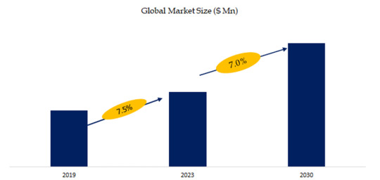
According to the new market research report “Global Polymer CMP Pads Market Report 2023-2030”, published by QYResearch, the global Polymer CMP Pads market size is projected to reach USD 1.38 billion by 2030, at a CAGR of 7.0% during the forecast period.
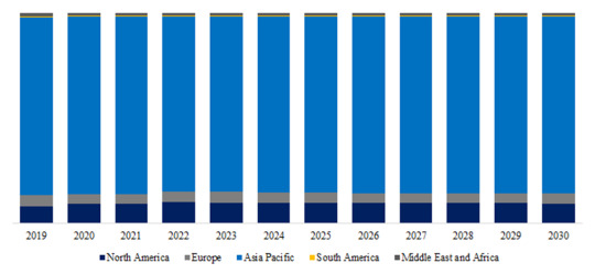
Figure. Global Polymer CMP Pads Market Size (US$ Million), 2019-2030
Above data is based on report from QYResearch: Global Polymer CMP Pads Market Report 2023-2030 (published in 2024). If you need the latest data, plaese contact QYResearch.
Figure. Global Polymer CMP Pads Top 10 Players Ranking and Market Share (Ranking is based on the revenue of 2023, continually updated)

Above data is based on report from QYResearch: Global Polymer CMP Pads Market Report 2023-2030 (published in 2024). If you need the latest data, plaese contact QYResearch.
According to QYResearch Top Players Research Center, the global key manufacturers of Polymer CMP Pads include DuPont, Entegris, etc. In 2023, the global top three players had a share approximately 82.0% in terms of revenue.
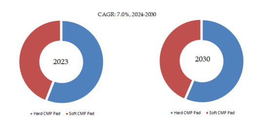
Figure. Polymer CMP Pads, Global Market Size, Split by Product Segment
Based on or includes research from QYResearch: Global Polymer CMP Pads Market Report 2023-2030.
In terms of product type, Hard CMP Pad is the largest segment, hold a share of 55.9%,
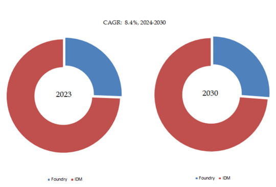
Figure. Polymer CMP Pads, Global Market Size, Split by Application Segment
Based on or includes research from QYResearch: Global Polymer CMP Pads Market Report 2023-2030.
In terms of product application, IDM is the largest application, hold a share of 74.6%,
Figure. Polymer CMP Pads, Global Market Size, Split by Region
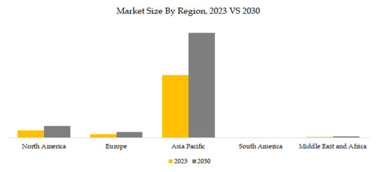
Based on or includes research from QYResearch: Global Polymer CMP Pads Market Report 2023-2030.
Market Drivers:
D1: The development of wafers has driven the development of its entire industrial chain, such as wafer shippers and carriers, wafer probe station, wafer bonding machine wafer grinder, electrostatic chucks, etc.
The development of the semiconductor industry has a continuous demand for wafer. Global achieved 9.28 billion USD from wafer, approximately 4% growth rate in the past few years.
The development of wafers will inevitably lead to the development of CMP polishing pads
D2: As a basic, leading and strategic pillar industry related to the overall national economy and social development, the semiconductor industry is strongly supported by various national policies. Among them, the huge localized replacement demand for core process materials in the semiconductor industry has become the general consensus of the market and the industry, showing a good situation of rapid growth. Benefited from the country's support for the semiconductor material industry and the rise of a number of companies in South Korea and China, the companies that started mass production in 2018 include South Korea's SKC (research and development and trial production before 2016) and Hubei Dinglong. These companies are expected to invest heavily in CMP polishing pads, and local companies will replace a large number of imported products.
D3: At present, advanced international chip manufacturers have used the 7-nanometer process technology, and the difficulty can be imagined. CMP enables chip manufacturers to continue to shrink circuit area and expand the performance of lithography tools. China and South Korea are countries with strong demand for CMP polishing pads. In the past, almost all CMP polishing pads in these countries depended on imports. After several years of development, the polishing pad technology of local manufacturers has the ability to replace overseas products. And local companies are expanding production on a large scale to replace imported products.
Restraint:
R1: CMP polishing pad is a key material in wafer polishing, and there is no alternative product. In addition, the market concentration of this industry is very high, and the suppliers are relatively stable. Furthermore, the product development and production costs are high and belong to a technology monopoly industry. So downstream customers have no bargaining power, but suppliers have strong bargaining power.
R2: The industry has a high technical threshold. New entrants must have a high level of technology, strong capital, broad sales channels, and the support of national policies to bring certain threats to leading companies. With the Japan-Korea trade war, the China–United States trade war continues to heat up. New entrants from China and South Korea expanded rapidly with the strong support of national policies, strengthened local brands to replace imported brands, and grabbed a certain market share.
Challenges:
C1: Trade deficits and disputes are the nodes that must be encountered for the rapid rise of national leading enterprises. During the trade war between Japan and South Korea, the Korean semiconductor industry was locked in the throat of fate because Japan restricted the export of key semiconductor materials. As a result, semiconductor materials have become the focus of attention from all walks of life. Korean domestic companies are facing great challenges. For example, FNS TECH Co., LTD, SKC is rapidly expanding production capacity. During the China–United States trade war, Hubei Dinglong Co., Ltd., a leading Chinese company, has increased its R&D and production of CMP polishing pads, expanded with the trend, and occupied a place.
C2: The raw material of Hard CMP Pad is mainly polyurethane, and the price fluctuation of raw materials has a certain impact on Hard CMP Pad. Considering the cost impact of all aspects, companies generally choose to purchase raw materials nearby.
C3: Under the influence of COVID-19, the global economy is declining. In the June report of the International Monetary Fund (IMF), almost all IMF member countries have lowered their predicted economic growth rates in 2020. In 2020, more than 95% of the country’s per capita income is expected to show negative growth, and the economic performance of export-oriented economies will be more severely affected.
About the Authors
Wei Qin
Lead Author
Semiconductor and Electronics
Email: [email protected]
About QYResearch
QYResearch founded in California, USA in 2007. It is a leading global market research and consulting company. With over 16 years’ experience and professional research team in various cities over the world QY Research focuses on management consulting, database and seminar services, IPO consulting, industry chain research and customized research to help our clients in providing non-linear revenue model and make them successful. We are globally recognized for our expansive portfolio of services, good corporate citizenship, and our strong commitment to sustainability. Up to now, we have cooperated with more than 60,000 clients across five continents. Let’s work closely with you and build a bold and better future.
QYResearch is a world-renowned large-scale consulting company. The industry covers various high-tech industry chain market segments, spanning the semiconductor industry chain (semiconductor equipment and parts, semiconductor materials, ICs, Foundry, packaging and testing, discrete devices, sensors, optoelectronic devices), photovoltaic industry chain (equipment, cells, modules, auxiliary material brackets, inverters, power station terminals), new energy automobile industry chain (batteries and materials, auto parts, batteries, motors, electronic control, automotive semiconductors, etc.), communication industry chain (communication system equipment, terminal equipment, electronic components, RF front-end, optical modules, 4G/5G/6G, broadband, IoT, digital economy, AI), advanced materials industry Chain (metal materials, polymer materials, ceramic materials, nano materials, etc.), machinery manufacturing industry chain (CNC machine tools, construction machinery, electrical machinery, 3C automation, industrial robots, lasers, industrial control, drones), food, beverages and pharmaceuticals, medical equipment, agriculture, etc.
0 notes
Text
0 notes
Text
0 notes
Text
How to Understand the Basics of Semiconductor Manufacturing by Nav Sooch
While semiconductor chips may appear small and insignificant, they're packed with powerful electronic components that seamlessly power our phones, laptops, and cars.
Semiconductor fabrication is an intricate and time-consuming process, and this article will introduce how semiconductors are constructed.
What is a Semiconductor?
Semiconductors are materials that conduct electricity partially, falling between an insulator like wood and pure conductors like copper. Semiconductors typically comprise crystalline materials like silicon; doping may alter their properties to produce integrated circuits or transistors with desired electrical characteristics.
Materials scientists define semiconductors as crystals with defects; to physicists, it has two energy bands called conduction band and valence band, which contain empty states where electrons can participate in current flow. To break through electron gridlock in the valence band, dopants must be added; their type will determine whether a semiconductor is N- or P-type.
Nav Sooch articulates that semiconductors can be found at the core of every electronic device, from space shuttles and electric cars to your everyday outlets and circuit breaker boxes at home. As these semiconductors form the backbone of our modern society and play an essential role in its prosperity and advancement, nations often compete to access superior semiconductors - which explains why many consider semiconductors "the world's most valuable raw material."
What is a Wafer?
Wafers are circular plates or discs used as the raw material for building integrated circuits (ICs). A wafer's surface contains die-square grids of electronic circuit elements forming its core - that make up its form.
Wafers are made from silicon that has been purified, melted, and cut into thin slices using diamond knives. Nav Sooch conveys that manufacturers then score along cleavage planes so that individual circuit elements can be diced off without using more material, known as wafer separation.
Wafers are then processed to form various layers and patterns of circuit elements, using multiple processes such as depositing metal (which can be accomplished via physical vapor deposition, chemical vapor deposition, electrochemical deposition, and molecular beam epitaxy), depositing metallic layers using patterning processes (physical vapor deposition), pattern etch processes (both wet and dry), patterning techniques and chemical mechanical planarization processes (CMP).
According to the insights of Nav Sooch, etching involves using either liquid or gas etchant to selectively remove portions of a wafer surface until desired circuit patterns remain behind. Patterning can then be completed using photolithography or electron-beam lithography.
Wafer test processes (also called sort or probe) occur on each patterned wafer, involving various testing procedures, including marking the die as good or bad and comparing it with other sorted wafers in an inventory die bank until customer demand arises for finished ICs.
What is a Die?
Die manufacturing is an essential step in the creation of microchips in smartphones. A die is a pre-formed tool used with a press to shape raw materials like plastic or metal with greater precision and functionality than molds could offer.
Die classification can take various forms, but one of the most accessible and valuable approaches is based on whether they're cutting or forming stock material. Any die that shears the material into pieces would be classified as a cutting die. At the same time, any that doesn't would fall under the developing die category - though remember that even those that perform both functions could fall under different classifications depending on how they're utilized.
Once a die has been created, it's placed inside a die press and subject to immense pressure, causing it to perform as intended - cutting material into specific finished shapes as indicated by its 'die line' in proofs.
As per Nav Sooch, die features to keep in mind include a stripper plate (to separate the workpiece from the die after every stroke), guide pins and pressure plates to spread the force across an entire piece, as well as various coining and drawing die types that use similar tools but accomplish different jobs. Nav Sooch Marriage
What is a Chip?
A chip is a fingernail-sized wafer of semiconductor material embedded with integrated circuitry that powers millions of devices like computers, cellphones, medical equipment, and appliances. Semiconductors are essential in the Fourth Industrial Revolution (4IR), making them integral parts of global economies worldwide. Nav Sooch highlights that semiconductor manufacturers form an important sector within global economies.
Silicon crystal is the primary component of semiconductor devices. Still, pure silicon may not provide optimal conductivity in various electrical applications, so phosphorus or boron may be added in small amounts for additional N-type or P-type semiconductor formation. Applying hostile voltage forces electrons through this semiconductor, creating an electric current with quantifiable results. Nav Sooch Marriage
ICs contain numerous transistors arranged in patterns on an integrated circuit chip. When a positive voltage is applied to the chip, this causes its transistors to turn on and deliver an electric current through it - acting like an electrical circuit and capable of performing complex tasks based on input from sensors or memory.
Once a chip is ready for sale, it must be packaged and sold as an individual unit. A typical package contains a label with the manufacturer's name or logo, part number information, four-digit date codes, and any details regarding its electrical specifications.
0 notes
Text
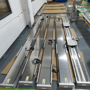
Linear Motor Actuators Will be Delivered to Germany
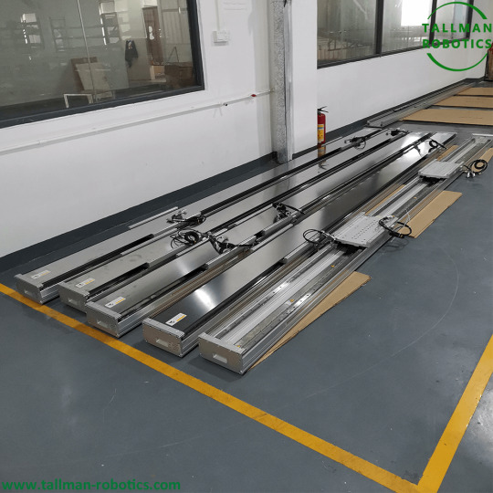
Linear Motor and Actuators from Tallman Robotics Will be Delivered to Germany.
Here are some details about linear servo motor modules:
1. Types of Linear servo Motors: Linear motor modules can be categorized into different types based on their design and configuration:
- Single-Axis Linear Motors: These actuators provide linear motion along a single axis. They are commonly used for applications that require linear positioning or pushing/pulling tasks.
-Multi-Axis Linear Motors: These actuators consist of multiple linear motors combined in a coordinated manner to provide motion in multiple axes. They are used in applications that require precise and synchronized movements in different directions, such as robotics or multi-axis machining.
- Planar Linear Motors: Planar linear motor modules are designed to provide motion in a two-dimensional plane. They can offer linear motion in both X and Y axes, making them suitable for applications such as gantry systems or XY tables.
- Curved Linear servo Motors: Curved linear motor modules are designed to provide linear motion along a curved path. They are used in applications that require motion along curved surfaces or tracks, such as in packaging or material handling systems.
2. Feedback Systems: Linear motor actuators often incorporate feedback systems to provide accurate position control and feedback information. These feedback systems can include optical encoders, linear scales, or Hall effect sensors. The feedback signals are used by the control system to ensure precise positioning and closed-loop control of the actuator.
3. Control Options: Linear motor actuators can be controlled in various ways depending on the application requirements. They can be controlled manually using switches or buttons, or they can be integrated into automated control systems. Automated control options include using programmable logic controllers (PLCs), motion controllers, or computer-based control systems. These control systems allow for precise control of motion parameters such as speed, acceleration, deceleration, and position.
4. Environmental Considerations: Linear motors can be designed to meet specific environmental requirements. For example, they can be built to withstand harsh conditions such as extreme temperatures, humidity, or exposure to dust or chemicals. This makes them suitable for applications in industries such as automotive, aerospace, or manufacturing where environmental conditions can be challenging.
5. Integration with Other Systems: Linear motors can be easily integrated with other systems or components to create complete motion solutions. They can be combined with mechanical components such as guide rails, bearings, or couplings to ensure smooth and precise linear motion. Additionally, they can be integrated with control interfaces, communication protocols, or network systems to enable seamless integration into larger automation systems.
6. Safety Considerations: Safety features can be incorporated into linear motor actuators to ensure safe operation. These features may include emergency stop buttons, limit switches to prevent overtravel, position sensors for accurate positioning, or torque sensing to detect abnormal loads or obstructions.
7. Cost Considerations: The cost of linear motors can vary depending on factors such as the type of linear motor used, the size and load capacity of the actuator, the level of precision required, and additional features or customization. It is essential to consider the specific application requirements and balance them with the associated costs to determine the most suitable linear motor actuator solution.
You are welcome to https://www.youtube.com/@tallmanrobotics to watch our video centre for more projects or visit our website to check other series or load down e-catalogues for further technical data.
Read the full article
#ElectricLinearActuators#LinearDCmotors#Linearmagneticmotorsandactuators#LinearMotorActuator#LinearMotorActuators#Linearmotorsingleaxisrobots#LinearMotors&Actuators#motorisedlinearactuator#StepperMotorLinearActuators#TubularLinearMotors
0 notes
Text
Chemical Mechanical Planarization Market to Exceed USD 12 billion by 2031, Rising at a CAGR of 7.9%
The global Chemical Mechanical Planarization (CMP) market is projected to witness substantial growth from 2023 to 2031, driven by the increasing demand for advanced semiconductor manufacturing processes, the proliferation of electronic devices, and the expansion of the automotive and aerospace industries. CMP is a critical process used in semiconductor fabrication, optics, and other precision manufacturing industries to achieve ultra-flat and smooth surfaces.
The chemical mechanical planarization market was worth US$ 5.6 billion in 2021, and the market is projected to reach US$ 12 billion by 2031. Chemical mechanical planarization sales are projected to increase at a CAGR of 7.9% until 2031.
A critical part of manufacturing MEMS devices is the manufacturing process of the CMP, which is used widely across several industries, including consumer electronics, automotive, healthcare, and industrial applications. A major driving force behind the growth of the CMP market is the development of MEMS technologies.
Get Access to Sample Research Report with Latest Industry Insights @ https://www.transparencymarketresearch.com/sample/sample.php?flag=S&rep_id=19007
Market Segmentation:
The CMP market can be segmented based on several factors including service type, sourcing type, application, industry vertical, and region. Understanding these segments facilitates a detailed analysis of specific market trends and dynamics.
By Service Type: Equipment, Consumables (Abrasive, Pad, Slurry)
By Sourcing Type: In-house, Outsourced
By Application: Semiconductor Manufacturing, Optics, Data Storage, MEMS, Others
By Industry Vertical: Electronics, Automotive, Aerospace, Healthcare, Others
By Region: North America, Europe, Asia-Pacific, Latin America, Middle East & Africa
Regional Analysis:
North America: Leading market due to the presence of key semiconductor manufacturers, technological advancements, and increasing investments in R&D.
Europe: Significant market share attributed to the growing automotive and aerospace industries and the increasing demand for high-performance electronic devices.
Asia-Pacific: Emerging market with rapid industrialization, extensive semiconductor manufacturing activities, and significant investments in infrastructure development.
Latin America: Growing adoption of CMP technology in electronics manufacturing and increasing investments in semiconductor fabrication facilities.
Middle East & Africa: Rising demand for advanced electronics and semiconductor components driving market growth in the region.
Market Drivers and Challenges:
Drivers:
Increasing demand for high-performance electronic devices and advanced optics.
Continuous advancements in semiconductor manufacturing processes.
Growing applications of CMP in emerging technologies such as 3D integration and MEMS.
Challenges:
Technological complexities associated with achieving ultra-flat and smooth surfaces.
Environmental and safety concerns related to chemical usage in CMP processes.
Intense competition from alternative surface finishing technologies.
Market Trends:
Integration of CMP with advanced process control technologies for enhanced precision and efficiency.
Development of next-generation CMP slurries and pads for improved material removal rates and surface quality.
Adoption of CMP in novel applications such as compound semiconductor manufacturing and advanced packaging.
Future Outlook:
The future outlook for the CMP market appears promising, driven by the increasing demand for high-performance electronic devices, advancements in semiconductor manufacturing processes, and the growing adoption of CMP in emerging applications. Market players are expected to leverage technological innovations and strategic partnerships to capitalize on evolving market trends and gain a competitive edge.
Key Market Study Points:
Analysis of market dynamics including drivers, challenges, and opportunities.
Assessment of market segmentation and regional trends.
Evaluation of competitive landscape and key market players.
Examination of recent developments and emerging trends shaping the market.
Competitive Landscape:
The CMP market is characterized by intense competition among key players striving to enhance their market presence through product innovation, strategic partnerships, and expansion strategies. Major players in the market include:
Applied Materials, Inc.
Ebara Corporation
Cabot Microelectronics Corporation
Entegris, Inc.
Fujimi Incorporated
Recent Developments:
Launch of advanced CMP equipment and consumables catering to specific customer requirements.
Strategic collaborations with semiconductor manufacturers and research institutions to drive innovation.
Investments in R&D to develop next-generation CMP technologies and materials.
Place an Order Copy of Chemical Mechanical Planarization Market Report at: https://www.transparencymarketresearch.com/checkout.php?rep_id=19007<ype=S
About Transparency Market Research
Transparency Market Research, a global market research company registered at Wilmington, Delaware, United States, provides custom research and consulting services. Our exclusive blend of quantitative forecasting and trends analysis provides forward-looking insights for thousands of decision makers. Our experienced team of Analysts, Researchers, and Consultants use proprietary data sources and various tools & techniques to gather and analyses information.
Our data repository is continuously updated and revised by a team of research experts, so that it always reflects the latest trends and information. With a broad research and analysis capability, Transparency Market Research employs rigorous primary and secondary research techniques in developing distinctive data sets and research material for business reports.
Contact:
Transparency Market Research Inc.
CORPORATE HEADQUARTER DOWNTOWN,
1000 N. West Street,
Suite 1200, Wilmington, Delaware 19801 USA
Tel: +1-518-618-1030
USA - Canada Toll Free: 866-552-3453
Website: https://www.transparencymarketresearch.com
0 notes
Text
Electronic Grade Hydrogen Peroxide Market Global Demand Analysis & Opportunity Outlook 2035
research analysis on “Electronic Grade Hydrogen Peroxide Market: Global Demand Analysis & Opportunity Outlook 2035” delivers a detailed competitor’s analysis and a detailed overview of the global electronic grade hydrogen peroxide market in terms of market segmentation by primary function, application, concentration and by region.
Economies of Gauge in Electric Creation to Promote Global Market Share of Electronic Grade Hydrogen Peroxide
In the fiercely competitive electronics market, manufacturers are searching for innovative ways to grow their market share and presence by providing cutting-edge products at lower prices through shorter lead times, with better product quality and more performance. A rising need for inexpensive electronic component removal from printed circuit boards is another factor driving the industry.
Due to the higher requirement for efficient and high-speed processing with smaller size, there have been more process stages added to the chemical mechanical planarization process in order to provide a crystalline silicon water surface. Hydrogen peroxide has been chosen by semiconductor manufacturers as one of their disinfection agents due to its strong disinfectant capabilities. This element is supporting the market.
Some of the major growth factors and challenges that are associated with the growth of the global electronic grade hydrogen peroxide market are:
Growth Drivers:
Increasing Demand for Etch ICs
Increased Use of Electronic Grade Hydrogen Peroxide in Paper and Pulp Industry
Challenges:
The biggest disadvantage of employing hydrogen peroxide products is that they can be extremely hazardous to handle if they contain more hydrogen peroxide than 3%. This substance may be harmful to the skin, eyes, and respiratory system due to its potent oxidative properties. A prolonged exposure may cause eye discomfort and hair bleaching.
Access our detailed report at:
By primary function, the global electronic grade hydrogen peroxide market is divided into four parts i.e., etchant, oxidizing, bleaching and cleaning agent. Out of these four categories, bleaching is expected to hold the largest share in the market. The substance is used in numerous industries, including textiles and medicine. Additionally, it is widely used as a whitening agent in the field of dentistry. In addition to being used as a mouthwash to maintain oral hygiene, it is used to bleach hair. A bigger percentage are used in the textile industry, where it is used to clean textiles and remove stains.
Asia pacific is expected to hold the largest market share. In 2021 the region, consisting of fast-growing economies such as India, China, South Korea and Indonesia, accounted for a 46.1 % global market share in industrial hydrogen. This growth has been facilitated by quick industrialization and increased demand from the end-use industries. Most of the major players in this market have their eyes on developing nations in the Asia-Pacific region, and they are steadily growing their manufacturing and research & development footprints. In Asia Pacific, the market is expanding as a result of rapid economic expansion.
Due to the long-term prevalence of water-borne illnesses in the region, North America is seen as being at the forefront of the wastewater treatment sector. Every day, the U.S. purifies more than 34 billion gallons of contaminated water to make it safe for locals to drink. One of the main requirements in the nation is the removal of phosphorus and nitrogen from water sources, along with the oxidation of wastewater. This has ultimately resulted in a significant use of hydrogen peroxide throughout the nation's industries.
This report also provides the existing competitive scenario of some of the key players of the global electronic grade hydrogen peroxide market which includes company profiling of Arkema Inc., Evonik Industries AG, PeroxyChem LLC, Chang Chun Companies, Aditya Birla Chemicals, Mitsubishi Gas Chemical Company, Akzo Nobel N.V., Kemira Oyj, OCI Company Ltd. and others.
Request Report Sample@
0 notes
Text
0 notes
Text
0 notes
Text
Europe Chemical Mechanical Planarization (CMP) Market Share, Size - Verified Industry Insights
Our Verified Industry Insights report on the Global Europe Chemical Mechanical Planarization (CMP) Market is an invaluable source of information for stakeholders in the market. Our report provides an in-depth analysis of the current market outlook, opportunities, and trends and also offers a comprehensive overview of the market including historical data, market size, and forecast as well. It also provides an overview of the major market players in the market and their competitive landscape.
Europe Chemical Mechanical Planarization (CMP) Market was valued at USD 1.71 Billion in 2022 and is estimated to reach USD 3.86 Billion by 2030, growing with a CAGR of 7.36% from 2023 to 2030.
The report also offers an in-depth analysis of the latest industry developments, such as new product launches, mergers & acquisitions, strategic collaborations, and partnerships with other market players. Furthermore, the report also provides an inside look at the competitive landscape and a detailed assessment of the market segments to help stakeholders make informed decisions. Additionally, the report offers insights into the industry dynamics which can help readers to understand the forces acting upon the market and the factors driving its growth. With the help of this report, our readers can gain comprehensive and reliable insights into the Global Europe Chemical Mechanical Planarization (CMP) Market.
Get a Sample PDF copy of this Europe Chemical Mechanical Planarization (CMP) Market Report:
Europe Chemical Mechanical Planarization (CMP) Market report also includes a pricing analysis for each type, manufacturer, region, and global price from 2018 to 2030. This information will help stakeholders make informed decisions and develop effective strategies for growth. The report's analysis of the restraints in the market is crucial for strategic planning as it helps stakeholders understand the challenges that could hinder growth.
This information will enable stakeholders to devise effective strategies to overcome these challenges and capitalize on the opportunities presented by the growing market. Furthermore, the report incorporates the opinions of market experts to provide valuable insights into the market's dynamics. This information will help stakeholders gain a better understanding of the market and make informed decisions.
Major Players Covered in this Report are:
Applied Materials Europe, Dialog Semiconductor, ASM, SUSS MicroTec, VDL enabling technologies, Horiba, Ebara Corporation, Lapmaster Wolters GmbH, LAM Research Corporation, Strasbaugh Inc.
One of the important sections of the research study includes the company profiling of key figures of the Europe Chemical Mechanical Planarization (CMP) Market. The authors of the report closely analyze all of the leading companies considered for the research study on the basis of different factors such as their main business, gross margin, and markets served. They also consider their prices, revenue, and production apart from the specification and application of their products. The review period considered here is of nine years.
Global Europe Chemical Mechanical Planarization (CMP) Market Segmentation Analysis
The outbreak of COVID-19 has dramatically changed the Europe Chemical Mechanical Planarization (CMP) Market. Worldwide, the industry saw signs of recovery in the second quarter, but the industry remains concerned about the prospects of long-term recovery as COVID-19 cases continue to rise, especially in Asian countries such as India.
Europe Chemical Mechanical Planarization (CMP) Market, By Type
CMP Consumables
CMP Devices
Europe Chemical Mechanical Planarization (CMP) Market, By Technology
Emerging
More than Moore
Leading edge
Europe Chemical Mechanical Planarization (CMP) Market, By Application
Compound Semiconductors
Integrated Circuits
Optics
Mems & Nems
Since the start of the pandemic, the industry received a series of blows and surprises. The pandemic has also led to many changes in buyer behavior and attitude. Thus, it is putting additional stress on the industry. This, in turn, is expected to restrain the growth of the market.
Some of the Key Questions Answered in this Report:
What is the Europe Chemical Mechanical Planarization (CMP) Market size at the regional and country-level
What are the key drivers, restraints, opportunities, and challenges of the Europe Chemical Mechanical Planarization (CMP) Market , and how they are expected to impact the market
What is the global (North America, Europe, Asia-Pacific, Latin America, Middle East, and Africa) sales value, production value, consumption value, import and export of Europe Chemical Mechanical Planarization (CMP) Market
Who are the global key manufacturers of the Europe Chemical Mechanical Planarization (CMP) Market? How is their operating situation (capacity, production, sales, price, cost, gross, and revenue)
What are the Europe Chemical Mechanical Planarization (CMP) Market opportunities and threats faced by the vendors in the Europe Chemical Mechanical Planarization (CMP) Market?
Which application/end-user or product type may seek incremental growth prospects? What is the market share of each type and application?
What focused approach and constraints are holding the Europe Chemical Mechanical Planarization (CMP) Market?
What are the different sales, marketing, and distribution channels in the global industry?
What are the key market trends impacting the growth of Europe Chemical Mechanical Planarization (CMP) Market ?
Economic Impact on the Europe Chemical Mechanical Planarization (CMP) Market and development trend of the Europe Chemical Mechanical Planarization (CMP) Market
What are the Europe Chemical Mechanical Planarization (CMP) Market opportunities, market risk, and market overview of the Atorvastatin Calcium market
Each chapter of the report provides detailed information for readers to understand the Europe Chemical Mechanical Planarization (CMP) Market further:
Chapter 1: Europe Chemical Mechanical Planarization (CMP) Market Product Definition, Product Types, Volume, and Revenue Analysis of Each Type in North America, Europe, Asia-Pacific, Latin America, Middle East, and Africa from 2023 to 2030.
Chapter 2: Manufacturer Competition Status, including Sales and Revenue comparison, Manufacturers' commercial date of Europe Chemical Mechanical Planarization (CMP) Market, product type offered by each manufacturer, Mergers & Acquisitions activities, and Expansion activities that occurred in the Europe Chemical Mechanical Planarization (CMP) Market.
Chapter 3: Europe Chemical Mechanical Planarization (CMP) Market Historical (2023-2030) and Forecast (2023-2030) Volume and revenue analysis of Europe Chemical Mechanical Planarization (CMP) Market in North America, Europe, Asia-Pacific, Latin America, Middle East, and Africa.
Chapter 4: Europe Chemical Mechanical Planarization (CMP) Market Product Application, Volume, and Revenue Analysis of Each Application in North America, Europe, Asia-Pacific, Latin America, Middle East, and Africa from 2023 to 2030.
Chapter 5 to 9: Europe Chemical Mechanical Planarization (CMP) Market Country Level analysis of North America, Europe, Asia-Pacific, Latin America, Middle East, and Africa, including volume and revenue analysis.
Chapter 10: Manufacturers' Outline, covering the company's basic information like headquarter, contact information, major business, Europe Chemical Mechanical Planarization (CMP) Market introduction, etc. Europe Chemical Mechanical Planarization (CMP) Market Sales, Revenue, Price, and Gross Margin of each company, as well as Recent Developments, are also contained in this part.
Chapter 11: Industry chains, like raw materials, and manufacturing costs, are covered. In addition, market opportunities and challenges are emphasized as well in the chapter.
Chapter 12: Market Channels, Distributors, and Customers are listed.
Chapter 13: Verified Market Reports Conclusions of Europe Chemical Mechanical Planarization (CMP) Market based on comprehensive survey.
Chapter 14: Methodology and Data Sources.
About Us: Verified Industry Insights
Verified Industry Insights is a leading Global Research and Consulting firm servicing over 5000+ global clients. We provide advanced analytical research solutions while offering information-enriched research studies.
We also offer insights into strategic and growth analyses and data necessary to achieve corporate goals and critical revenue decisions.
Our 250 Analysts and SMEs offer a high level of expertise in data collection and governance using industrial techniques to collect and analyze data on more than 25,000 high-impact and niche markets. Our analysts are trained to combine modern data collection techniques, superior research methodology, expertise, and years of collective experience to produce informative and accurate research.
Our research spans a multitude of industries including Energy, Technology, Manufacturing and Construction, Chemicals and Materials, Food and Beverages, etc. Having serviced many Fortune 2000 organizations, we bring a rich and reliable experience covering all research needs.
Contact us:
Mr. Edwyne Fernandes
US: +1 (650)-781-4080
US Toll-Free: +1 (800)-782-1768
0 notes
Link
0 notes
Text
All the basics that you should know about stainless steel.
A flange is required whenever two tubes are connected to one another. It is utilized in the process of threading or welding the ends of two tubes together to create a single connected tube. Therefore, depending on the technique of attachment that is employed, fasteners can be generically categorized as either threaded attachment flanges or welding flanges. When it is time to link two tubes together, a flange junction has to be assembled using a gasket, many bolts and nuts, and a set of flanges.
To begin, place the gasket so that it is sandwiched between the mating sides of your seal. The screws then need to be tightened. When the gasket's surface pressure reaches a certain value, it deforms to completely conceal any inconsistencies in the sealing surface. The makers of PVC coated stainless steel tubing have consistently been a dependable resource.
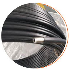
Flange joints are a type of interchangeable connection. Flanges for both containers and tubes are available as interchangeable parts. Stainless steel sanitary tubing suppliers might be of great assistance.
There are three different types of sealing faces, depending on the pressure and the type of media being sealed against: planar sealing faces for low pressure, uneven sealing faces for moderate pressure, and tongue and groove sealing faces for high pressure and combustible, explosive, and toxic media. One such choice is ss capillary tubes manufacturers in India.
Different flanges can withstand different pressures and media, as you know. It turns out that the gasket utilized in the connection is crucial. Non-metallic plates in particular have been used to produce an abundance of gaskets. The stainless steel coil tubing manufacturers has been outstanding.
Asbestos rubber sheets, asbestos plates, polyethylene table sheets, and so on all have sizes that are specified in various standards. A latex gasket, for example, can only withstand temperatures up to 120? Asbestos with a high acid-resistance content has been widely used in harsh environments. Copper, aluminum, 10 steel, or stainless steel sheet metal is necessary in the event of increased pressure. India is home to a plethora of top-notch stainless steel boiler tube manufacturers.
Despite their apparent simplicity, fasteners have become more important in virtually every industry because of the vital roles they play. The two are joined by the fasteners. These days, the majority of individuals prefer to make use of them.
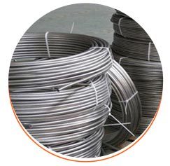
Flange, in reality, follows its own set of guidelines. The three systems in question are the DIN system, the ANSI scheme, and the JIS system. Similar pressure thresholds and sealing face types are needed for both systems. Stainless steel condenser tube manufacturers are highly sought after by a majority of customers nowadays.
Furthermore, the latter method is not generally accepted. Additionally, the GB standard, the chemical standard, the mechanical standard, and the pressure vessel benchmark should all be followed during production of the flanges. Industrial processes rely heavily on pipes and tubes as well. These technological advancements accommodate for human limitations by carrying out activities that humans are unable do.
0 notes
Text
Post CMP Cleaning Market Size, Emerging Trends, Technological Advancements, and Business Strategies 2023-2032
The global Post CMP Cleaning market was valued at US$ 193.6 million in 2022 and is projected to reach US$ 319.8 million by 2029, at a CAGR of 7.4% during the forecast period. The influence of COVID-19 and the Russia-Ukraine War were considered while estimating market sizes..
Get Full Report @ https://semiconductorinsight.com/report/post-cmp-cleaning-market-size-emerging-trends-technological-advancements-and-business-strategies-2023-2032/
Post CMP cleaning refers to the process of removing particles, residues, and contaminants from the surface of a substrate after undergoing chemical mechanical planarization (CMP). CMP is a critical step in the manufacturing of semiconductors, where it is used to create a flat and smooth surface on the substrate.
While CMP is essential for achieving the desired substrate surface, it often leaves behind residues that can negatively impact the performance and reliability of the semiconductor. Post CMP cleaning is therefore employed to effectively eliminate these residues and ensure the quality of the semiconductor.
The cleaning process typically involves using specialized cleaning solutions or chemicals, such as acidic or alkaline cleaners, to remove the residues and particles. Various techniques may be utilized, including ultrasonic cleaning, plasma cleaning, or electrochemical cleaning, depending on the specific requirements and characteristics of the semiconductor.
Post CMP cleaning plays a crucial role in enhancing the yield and functionality of semiconductors, as it ensures the cleanliness and integrity of the substrate surface. By removing any contaminants left behind by the CMP process, post CMP cleaning contributes to the overall quality and performance of the final semiconductor product.
This report aims to provide a comprehensive presentation of the global market for Post CMP Cleaning, with both quantitative and qualitative analysis, to help readers develop business/growth strategies, assess the market competitive situation, analyze their position in the current marketplace, and make informed business decisions regarding Post CMP Cleaning.
The demand for high-performance integrated circuits (ICs) is on the rise across various applications, including smartphones, tablets, laptops, and servers. These applications require ICs that offer high speed, low power consumption, and exceptional reliability. Post CMP cleaning plays a critical role in ensuring the optimal performance and reliability of these ICs.
To meet the evolving needs, there is an ongoing development of new post CMP cleaning technologies. These emerging technologies aim to enhance the effectiveness of residue and particle removal. Among the approaches being explored are ultrasonic cleaning, plasma cleaning, and electrochemical cleaning, which hold promise for improved cleaning capabilities.
In addition to technological advancements, there is a growing demand for sustainable post CMP cleaning solutions. Industry stakeholders are seeking environmentally friendly alternatives that minimize or eliminate harmful emissions. This growing focus on sustainability has spurred the development of post CMP cleaning solutions based on eco-friendly solvents and chemicals, ensuring both effective cleaning and environmental responsibility.
This report contains market size and forecasts of Post CMP Cleaning in global, including the following market information:
Global Post CMP Cleaning Market Revenue, 2018-2023, 2024-2029, ($ millions)
Global Post CMP Cleaning Market Sales, 2018-2023, 2024-2029, (Tons)
Global top five Post CMP Cleaning companies in 2022 (%)
Global key players of post CMP cleaning include Entegris, Versum Materials (Merck KGaA), Mitsubishi Chemical, Fujifilm, etc. Global top five manufacturers hold a share over 77%. North America is the largest producer of post CMP cleaning holds a share over 55%. In terms of product, acidic material is the largest segment, with a share over 53%. And in terms of application, the largest application is metal impurities and particles, with a share over 68%.
The surge in demand for semiconductors across a variety of industries like electronics, telecommunications, and automotive is the primary driving force behind the market. This increasing need for high-performance semiconductors has led to a corresponding rise in demand for post CMP cleaning solutions.
Post CMP cleaning is a crucial process used to eliminate particles, residues, and contaminants from the substrate after undergoing chemical mechanical planarization (CMP). CMP is a vital step in semiconductor manufacturing, as it helps achieve a smooth and even substrate surface. However, CMP also leaves behind residues that can negatively impact semiconductor performance. The purpose of post CMP cleaning is to eradicate these residues and ensure the overall quality of the semiconductor.
The market for post CMP cleaning is categorized based on product type, application, and geography. In terms of product type, the market consists of acidic cleaners, alkaline cleaners, and solvent-based cleaners. Acidic cleaners are the most widely employed type of post CMP cleaner due to their effectiveness in removing a broad range of residues. Alkaline cleaners are also utilized, although they may not be as effective as acidic cleaners when it comes to removing certain types of residues. Solvent-based cleaners, on the other hand, find application in specific scenarios such as cleaning hard disk drives.
We surveyed the Post CMP Cleaning manufacturers, suppliers, distributors and industry experts on this industry, involving the sales, revenue, demand, price change, product type, recent development and plan, industry trends, drivers, challenges, obstacles, and potential risks.
Total Market by Segment:
Global Post CMP Cleaning Market, by Type, 2018-2023, 2024-2029 ($ Millions) & (Tons)
Global Post CMP Cleaning Market Segment Percentages, by Type, 2022 (%)
Acidic Cleaners
Alkaline Cleaners
Solvent-based Cleaners
Global Post CMP Cleaning Market, by Application, 2018-2023, 2024-2029 ($ Millions) & (Tons)
Global Post CMP Cleaning Market Segment Percentages, by Application, 2022 (%)
Metal Impurities and Particles
Organic Residue
Electronics
Telecommunications
Automotive
Others
Global Post CMP Cleaning Market, By Region and Country, 2018-2023, 2024-2029 ($ Millions) & (Tons)
In 2022, North America emerged as the largest market for post CMP cleaning, capturing over 30% of the global market share. The region’s growth can be attributed to the significant presence of key semiconductor manufacturers like Intel, AMD, and Micron Technology. These industry leaders are actively investing in new product development and expanding their production capacities, thereby fueling the demand for post CMP cleaning solutions.
Europe holds the position of the second largest market, accounting for over 25% of the global market share in 2022. The growth in Europe is primarily driven by the escalating demand for semiconductors in the automotive and telecommunications sectors. The automotive industry, in particular, relies on semiconductors for diverse applications such as electronic control units (ECUs), power steering systems, and infotainment systems. Likewise, the telecommunications industry utilizes semiconductors for various purposes including base stations, routers, and switches.
As for the Asia Pacific region, it stands as the third largest market, commanding more than 20% of the global market share in 2022. The market’s expansion in this region can be attributed to the surging demand for semiconductors in the electronics and telecommunications industries. In the electronics sector, semiconductors find applications in popular devices like smartphones, tablets, and laptops. Similarly, the telecommunications industry relies on semiconductors for essential components such as base stations, routers, and switches.
The Rest of the World region secures the fourth position, accounting for over 25% of the global market share in 2022. The market’s growth in this region is fueled by the increasing demand for semiconductors in emerging markets like China, India, and Brazil. Among them, China holds the largest market share for semiconductors in the Rest of the World. The Indian market is experiencing rapid growth due to significant investments in the electronics and telecommunications sectors. Additionally, the Brazilian market is expanding as a result of increased investments in the automotive and telecommunications industries.
Global Post CMP Cleaning Market Segment Percentages, By Region and Country, 2022 (%)
North America
U.S.
Canada
Europe
U.K.
Germany
France
Spain
Rest of Europe
Asia-Pacific
India
Japan
China
Australia
South Korea
Rest of Asia-Pacific
Latin America
Brazil
Mexico
Rest of Latin America
The Middle East & Africa
South Africa
GCC Countries
Rest of the Middle East & Africa (ME&A)
Further, the report presents profiles of competitors in the market, key players include:
Entegris
Versum Materials (Merck KGaA)
Mitsubishi Chemical
Fujifilm
DuPont
Kanto Chemical
BASF
Solexir
Anjimirco Shanghai
Honeywell International
Parker Hannifin
Technic
Solvay
Recent Developments:
Entegris introduced its latest post CMP cleaning solution, the IONCLEAN™ ICP Platform, in January 2023. This platform employs inductively coupled plasma (ICP) technology to effectively eliminate residues and particles from wafers. Designed specifically for the manufacturing of high-performance integrated circuits (ICs), the IONCLEAN™ ICP Platform offers an advanced solution for post CMP cleaning needs.
In February 2023, Versum Materials made an acquisition by purchasing Technic, a renowned provider of post CMP cleaning solutions. This strategic acquisition aims to expand Versum’s existing portfolio of post CMP cleaning solutions and reinforce its position in the market. By incorporating Technic’s expertise and offerings, Versum Materials can further cater to the diverse needs of customers seeking reliable post CMP cleaning solutions.
Fujifilm introduced its eco-friendly post CMP cleaning solution, the Eco-Clean™, in March 2023. This solution is built upon environmentally friendly solvents and chemicals, aligning with the rising demand for sustainable post CMP cleaning options. With its focus on environmental responsibility, Fujifilm’s Eco-Clean™ addresses the industry’s growing need for effective yet environmentally conscious post CMP cleaning solutions.
In April 2023, Mitsubishi Chemical Corporation launched the AquaSolv™ post CMP cleaning solution. This innovative solution utilizes a novel solvent technology that surpasses traditional solvents in effectively removing residues and particles. Mitsubishi Chemical Corporation’s AquaSolv™ caters to the industry’s demand for more efficient and reliable post CMP cleaning solutions, providing a cutting-edge option for manufacturers.
Get Full Report @ https://semiconductorinsight.com/report/post-cmp-cleaning-market-size-emerging-trends-technological-advancements-and-business-strategies-2023-2032/
0 notes
Last Seen Blogs

mandradekhol-blog
Alpha Genix XL

thebigsl33p
The Eternal Slumber

izaya-inuyasha
Inuyasha is my Origin

running-from-ashes
RUNNING FOR PEACE OF MIND

neonlights22
I want waffle fries-