
screenprotectorncase
Screen Protector, Case and Accessory
26 posts
Don't wanna be here? Send us removal request.
Last Seen Blogs

syronixq
Syron

karenfordonte
Caring For Donte

joonscore
ㄥ ֶָ֢

floramau
!! UNDEAD UNDEAD UNDEAD !!

ohmygzbcledits-blog
lee*
Photo

Protection case for Apple Watch, case with built-in 9H tempered glass, protecting Watch’s screen from scratch or broken.
Please email me if have interest, [email protected]
0 notes
Photo

protection case for your smart watch with built-in tempered glass #iwatch #case https://www.instagram.com/p/CNWR2u2jzSc/?igshid=epqc6avhfg4n
0 notes
Photo

99.99% Anti-Bacterial tempered glass screen protector, Japan SIAA certification.
Wholesale or distributor please email [email protected]
0 notes
Text
SIAA certificated Antibacterial and Anti-virus Screen Protector and Case
People pay more attention to those products carrying with antibacterial and anti-virus function because of the effect of Covid-19, not just because of the special epidemic, people only pay attention to sanitation in short period, we should always have the sense and the habit to protect ourselves from bacterial and virus. Smart phone as a close tool who stay with us most of the time of a day, easily be carried with bacterial and virus by being touching or placing somewhere. MBL company (Shenzhen Membrane Precise Electron Ltd) release screen protector and case with antibacterial and anti-virus function in 2020

We cooperated with a Japanese material company and develop it when the Covid-19 breaking out, successively launched 3 types product:
1. Antibacterial and Anti-virus protective PET film, which got Japanese SIAA certificated. (Member No.: 2422)
2. Antibacterial tempered glass, also got Japanese SIAA certificated. (Member No.: 2422)
3. Antibacterial and Anti-virus protective case.
Above products are MP and exporting to Japan.
Currently, we not only apply for mobile accessory products, but also deal with some projects such as lift button, ATM, vending machine...from other industry. We really highly appreciate those people who take care of our health and consider more then ourselves, e.g., when we taking a lift and pressing the button, then notice the button is covered with Antibacterial and Anti-virus protective film, we might feel safe, don't you?
Some of you might have question, will the antibacterial and anti-virus function be permanent? The answer of course is Yes!
For more detailed information, please feel free to connect us.
Tel: +86 0755-2967 2889 Email: [email protected]
0 notes
Text
Renice X5A industrial grade CFast 2.0 card

Renice releases their industrial grade CFast 2.0 card in April 2018, it is a compact storage card with SATAIII 6.0Gb/s interface, with the CFast 2.0 standard and ATA protocol, offering high performance, reliability and low power consumption to next generation embedded devices. Its maximum Read/Write speed up to 520/440 MB/s, maximum capacity up to 512GB (MLC), features with Power Failure Protection and Over Voltage Protection, optional functions including Hardware Write Protection and Write Protection. Comparing to X1 Plus CFast 1.0 card, the new X5A CFast card highlights on its speed, which is an ideal storage device for high speed camera, embedded computer (SBC) and data logger/recorder.
To learn more or want to ask for a quote, please feel free to email [email protected]
0 notes
Text
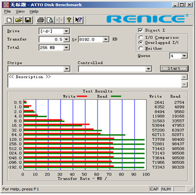
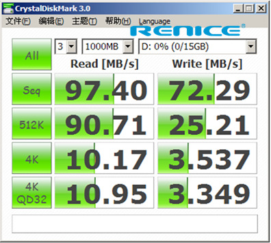
High Reliability Industrial grade CompactFlash Card
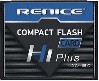
Renice H1 PLUS CompactFlash card adopts German Hyperstone controller solution, as know that Hyperstone controller highlights stability in harsh environment applications. Its max sequential data Read/Write speed up to 95MB/75MB/s, and with incredible 4K Read/Write performance (e.g: 16GB SLC, 4K R/W speed is 10.17MB/3.54MB/s), its max capacity can up to 512GB. Support hardware 96-Bit /1KB BCH ECC error correction and AES128 and AES256 support with CBC and XTS modes, high performance on-the-fly encryption/decryption.

The Renice Industrial CompactFlash H1 PLUS Memory Card meets the industrial reliability, endurance and functional requirements, design with power-down protection, secure erase and other special features. Advanced write-leveling, data-read immunity management and brown-out management provide the highest levels of stability and durability. Market-oriented groups are mainly in the field of industrial automation, embedded computing, industrial applications, network communications, public safety, military, aerospace, medical and automotive.
To learn more technical information please contact May Lau at [email protected].
0 notes
Text
Renice Rugged 3U 4TB 8TB LRMs storage module
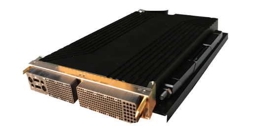
Renice 3U LRMs storage system is designed for Surveillance Aircraft, Rugged Computer, In-Vehicle applications, Video Surveillance etc.
The storage module has a capacity of 8TB and is suitable for military aircraft. It conforms to the reliability design guidelines for military aircraft. It uses Renice self-developed control chip SSD, to provide block-level file storage and retrieval services through the SAS interface. It has abnormal power-down data protection function and physical self-destruction and logic self-destruction function. The entire storage module adopts wide temperature design and super-strong LDPC+BCH mixed error correction algorithm, greatly improving product reliability, and making product lifetime more than three times than that of similar products in the market. It provides 8 channels of read/write 400MB/channel transmission performance, and ultra-high performance with a sequential write speed of more than 3000MB/sec on the entire disk, internally using military isolated power supplies.
To learn more technical information please connect May Lau at [email protected].
0 notes
Text
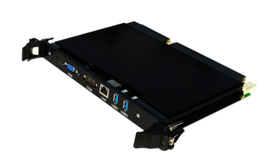
Renice 6U VPX Rugged Single Board Computer: CPU+GPU(GPGPU)

0 notes
Text
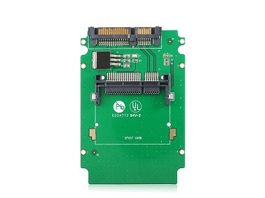
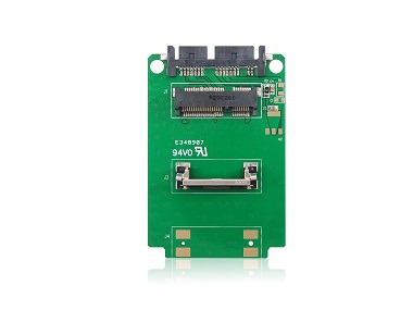
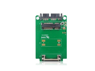
Renice industrial quality adapters: mSATA to 2.5" SATA Adapter, mSATA mini to 2.5" SATA Adapter, mSATA to 1.8" micro SATA Adapter, NGFF to 2.5" SATA Adapter, mSATA mini to 1.8" micro SATA adapter, CFast to 2.5" SATA Adapter. (USD$7 per/pc, [email protected])


0 notes
Text
סקירה: 16GB SLC כרטיס פלאש
רניס H1 Plus CompactFlash CF כרטיס, כרטיס תעשייתי כיתה Flash, אימצה הגרמני בקר Hyperstone פתרון, אשר מדגיש יציבות ביישומים הסביבה הקשה.איכותי 4K קריאה / כתיבה ביצועים קיבולת מקסימלית של עד 512GB.
0 notes
Text
Überprüfung: 16 GB SLC Flash-Karte
Renice H1 Plus CompactFlash CF-Karte, Industrie-Flash-Karte, deutsche deutsche Hyperstone-Controller-Lösung, die Stabilität in rauen Umgebungen Anwendungen unterstreicht. Unglaubliche 4K Read / Write-Leistung und maximale Kapazität von bis zu 512 GB.
0 notes
Text
Incredible 4K Read/Write performance, Renice industrial grade Compact flash memory card,up to 512GB
0 notes
Text
Nand Flash: SLC, MLC and TLC, how much do you know?
I do SSD drive business and deal with many RFQs related to SSD, but few customers know about the difference among SLC, MLC and TLC, so I have to explain every time, here I’d like to share something I know, hope it helps.
Part 1 - Principle of Nand Flash Storage

(Basic architecture of a Cell)
As we know that all the data store as “0” and “1” in computers, so in theory if the storage unit can provide two or more recognized status, it can be used for data recording.
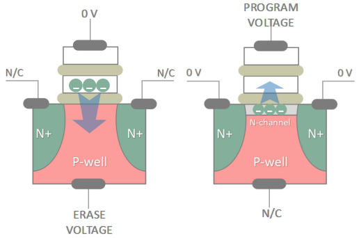
1. “Write” Data
When writing data, we need to apply high voltage to the Control Gate, and allowing electrons flows into the N-Channel which is between the Source and Drain, when the current is strong enough, electrons gain sufficient energy and then will cross the SiO2 layer (which is under the Floating Gate), finally being captured by the Cell, we call the whole process as “Tunnel Effect”.
2. Data Stabilization
Once the electrons enter into the Floating Gate, they can’t get away from the SiO2 layer if there is not enough energy, even turn off the power supply, then the statue of the electron capture will continue and could be last for years, of course it depends on the wear condition of SiO2 layer.
3. “Read” Data
When reading data, we also need to apply voltage to Control Gate in order to absorb the electrons in the Floating Gate, but it’s not necessary to apply voltage as high as its Tunnel Injection process. Meanwhile, let the current cross the N-Channel to detect the amount of electron capture in Floating Gate, convert to binary “0” &“1” based on the induction intensity, finally output the data.
4. “Erase” Data
If need to erase data, we won’t apply voltage to the Control Gate but to the P-well Current between the Source and Drain flows through the N-Channel and will react on electrons, then the electrons in the Floating Gate will cross the SiO2 layer again and be attracted in the opposite direction, that’s what we called “Tunnel Release”.
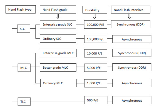
Part 2: Brief Introduction to SLC, MLC and TLC
1. Definition of SLC, MLC, TLC
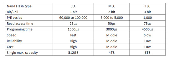
SLC (Single-Level Cell), means every single Cell only stores 1bit message, data output is based on the Yes or No status of electrons capture (even though it’s in the status of “0”, there are some electrons in the Floating Gate), which is what we call “0” and “1”.
MLC (Multi-Level Cell), means every single Cell can store 2bit message, the number of electrons in Floating Gate is divided into 4 conditions: High, Medium, Low and None, converted to binary and becomes 00, 01, 10 and 11.
TLC (Triple-Level Cell), the status of electrons capture in the Floating Gate is further divided into eight types then converted to binary and becomes 000, 001, 010, 011, 100, 101, 110 and 111, that’s what we call “3bit”.
2. SLC vs MLC
Five aspects (Lifespan, Cost, Power consumption and Error rate) to illustrate the main difference between SLC and MLC:
2.1 Lifespan
l Principles
Data storage in the SSDs depends on the amount of electrons captured by the Floating Gate in the Cell. No matter entering or leaving the Floating Gate, the electrons need to cross the SiO2 layer through Tunnel Effect behavior. Actually the thickness of SiO2 layer is only about 10nm, so the atomic bond of SiO2 will be destroyed little by little when doing Tunnel Injection or Tunnel Release operation. Therefore, the speed of data erasure will be slower, that’s because the electrons will occupy the SiO2 layer, and counteract the voltage which applied on the Control Gate, resulting in needing higher voltage to finish its task. By the time when the SiO2 layer is throughout by electrons, the Cell unit is officially dead.
l Conclusion
As know that the status of electrons capture of SLC only has two types, while MLC has four, in order to achieve at four kinds of status, the electrons in the MLC’s Cell unit need to frequently enter and leave the SiO2 layer, which leads to accelerate the depletion of the Cell, that’s also why SLC has 100,000 P/E cycles while MLC only has 10,000 P/E cycles.
Apperantly, TLC has the least P/E cycles, average 500 to 1000, which is usually used in USB stick.
2.2 Comparison in Speed, Power consumption, Reliability, Error rate and Cost
It’s very easy to , so when under the same controller chip and computational logic, the speed of SLC is the fastest, the lowest Power Consumption, the most stable performance, and the negligible error rate with the help of today’s technology.
A Cell unit of SLC only stores 1bit data, but MLC’s can store 2bit or more, the volume of MLC chip , that’s to say, MLC’s capacity gets higher than SLC (though they are the same chip), so MLC’s price is cheaper.
Since MLC and TLC highly rely on ECC (Error correction Coding), data will dramatically loss once error happens, but good news is that ECC technologies are quite mature till 2012.
2.3 Difference in storage capacity
For single Nnad flash, SLC max. up to 512GB, MLC up to 4TB, and TLC can up to 6TB (end by Aug-01-2017)
Part 3 – Nand Flash Classification
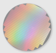
Wafer (see the above picture), each of the above squares can be made into a memory card. Not all the Die on the factory wafer is in superior quality, just like the Nand Flash who also has factory Bad Block. Take Intel and Micron for example (IM Flash Technology – IMFT is jointly owned by Intel and Micron)
(1) Some good Die can be used for high grade Synchronous Nand.
(2) Some will be used as inferior Synchronous Nand after repairing and verifying.
(3) And the low-grade asynchronous Nand might be used for memory cards.
So, do not be blinded by the brand Nand Flash, even Intel, Micron (no offence here), but you can judge the quality from their model number.
Part 4 - Synchronous and Asynchronous
The main difference between synchronous and synchronous Nand flash is their Pin definition, when in synchronous mode, Nand flash doesn’t need to tell the controller that “I’m ready for reading/writing”, but always be “Ready” status and time-saving.
e.g. Intel 25nm Nand flash Classification:
Renice's SSD adopts original industrial grade Intel/Micron Nand flash, and further sorting by our Nand Flash Analyzer NFA100 to select the best grade Nand flash in order to provide the most reliability SSD solution for our customers. To learn more, please email [email protected].
0 notes
Text
Military SSD vs Consumer SSD, Big difference!
The essential difference between military SSD and consumer SSD is their security and reliability, not the speed performance.
And What cause their security and reliability such a big difference? The answer is design idea and material selection!
The cost of SSDs differs from several times and even more, though using the same capacity and the same chipset, when adopting different design idea and material.
The design idea of consumer level SSD is performance prior and cost saving, for instance, when can use 4 layers, they won’t choose 6 layers, moreover, if some material can be omitted then they will leave out. While military SSD will put reliability in the first place, if 10 layers needed then 10 layers, and all the materials is military or industrial standard. Because of these different thinking, it makes big difference between consumer and military level SSD.
1. Working/Operation Temperature
Usually -40°C to +85°C, even -55°C to +125°C temperature range of military SSD is common requested, while consumer level SSD just request 0°C to 70°C working temperature range.
Under the low or high temperature environment, electric performance changes greatly, military SSD products have high standard on material selection, not only all electronic components must be industrial standard, but also require high requirements on PCB cabling and circuit board. As known, ordinary PCB will blister after highbake (e.g. 260°C) for more than 2 times, circuit board layers will be broken, which leads into poor connection. While the PCB of military SSD will not has such problem even under the same condition. How to judge the quality of PCB? The simple way is putting the PCB into a 260°C roaster undergoing and repeatedly baking for several times, until the PCB surface becomes pasted if no blister, then qualified.
2. Reinforcement Process
2.1 Glue
Firstly, the chipset of military SSD will be reinforced by glue, then will be solidified under 160°C heat. The glue not only connects the PCB with chipset, but also completely discharges the air of chipset pin, preventing the chipset pin from oxidating in the future, what’s more, waterproof.
(How to do? Rencie will use German brand glue and make each chipset glued through the robotsealing, tilted 45 °C for 30 minutes to let the glue automatically infiltrate until the air emptying, and then heating, the whole gluing process takes more than 1 hour.)
2.2 Rugged Connector
Usually ordinary SATA connector is planar contact structure, whose structure is simple manufacture and low cost, but if applied in lots of vibrations and jerks environment, such planar contact structure will have transient poor connection condition, then leads into signal disappear or data loss, therefore, military SSD will use special customized rugged SATA connector.
Internal structure of R-SATA connector:
This kind of rugged connector won’t have poor connection condition regardless of any direction of vibration and shock.
Of course, using rugged housing is another way of military SSD reinforcement.
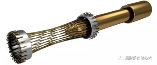
3. Push-to-trigger Destruction Function
Consumer level SSD doesn’t have requirement on some special functions, but military SSD does, data destruction is necessary in some conditions:
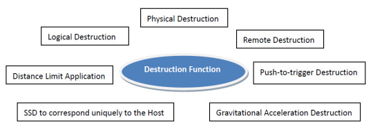
Physical destruction design is not just simply added some circuit, actually it’s hard to burn because the flash itself carries with circuit-protection feature, meanwhile, different Nand flash increase the difficulty of burning. Renice have done lots of test experiments and find out a way to ensure all the flash will be burned out.
http://www.renice-tech.com/html/2016/04/27/201604270301491655582064.html
4. Reliability
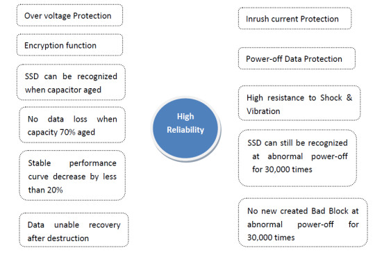
So we can see from the reliability of military SSD and find out that it needs to take a wide range of factors into consideration, and requires a lot of testing, debugging and verifying. While consumer grade SSD doesn’t need to go through these process.
Rugged SSD manufacturer: www.renice-tech.com
Consult: [email protected]
0 notes
Text
Power Failure/Loss Protection of SSD drives
SSD problems caused by power failure:
Generally power failure would cause 3 main problems to SSD when PC runs.
1. Mapping table might get lost because there is no enough time to update and store it. Usually SSD manufacturers do not provide users with tools to recover mapping table. Thus SSD will become undetectable to host and only method is to return the drive to manufacturer for repairing. And SSD vendors will reproduce the drives by firmware which will get all data on SSD lost.
2. SSD mostly deploy DDR or SDRAM as the cache on board. Once power fails, all data in cache will be lost because both DDR and SDRAM are non-volatile media. And these data have never been transferred into NAND flash yet because R/W speed of DDR is far higher than NAND Flash. However host will consider that data writing has already been finished. In this way power failure causes data loss.
3. Power failure results in new nominal bad blocks. ECC of controller checks 256bit data in row and column, and xor each bit(If result is 0, it means even numbers of 1. If result is 1, it means odd number of 1). When power failure occurs, there might be errors above 1 bit in 1 block, which cannot be corrected by ECC because it only deals with 1 bit’s error at 1 time. Then controller will misjudge this block as bad one and will not use it for new data storing. This is why common SSD tools find increased bad block numbers after power failure happens.
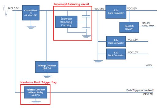
Renice solution:
Renice deploys super capacitor or tantalum capacitors on specific SSD models, and detect the input power from both capacitor’s and SATA power’s input end. Detection circuit is interfacing with corresponding GPIO so that abnormal signal of power will be reported to SSD Firmware through GPIO when power fails. When 5v power supply breaks off, SSD will report to HOST and stop to receive data not reaching SSD. Renice solution also takes over-current into consideration. Once the input current is detected to excess limitation, current-limiting circuit (Protection circuit to prevent damaging over components if instantaneous input current is too large) will report to SSD controller, as reactions original power supply will be cut off and capacitors will provide the power required to transfer mapping table and data in cache into NAND flash.
Validation methods:
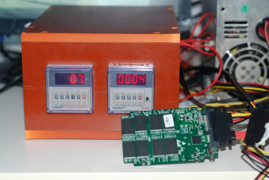
Renice’s engineer team developed our own instrument to produce power blackout in different operation process, including reading, writing, shutting down, starting up, rebooting, or even irregular power blackout.
Using this instrument Renice implements power on-off for 3,000 cycles to verify SSD’s power failure protection is able to run well in real trial.
www.renice-tech.com
0 notes