
Last Seen Blogs

zuri2235
Moon🌙

art-olotl
Is It Really You?

fitw91
Fashion Is The Weapon

indigomeow
proud dteamolo

samsung5575
Untitled
Quote
The story of the change of WeChat
http://en.folysky.com/p-article_detail/id-241.html
0 notes
Photo

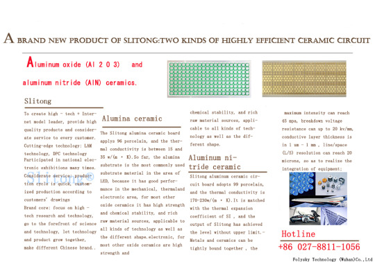
Aluminum Nitride Ceramic Circuit Board
0 notes
Link
0 notes
Photo

Ceramic substrate manufacturers ranking
Ceramic substrate (http://en.folysky.com)products come out, opening the development of heat radiation application industry,The ceramic substrate has the advantages of high heat dissipation, low heat resistance, long life and voltage resistance,With the improvement of production technology and equipment, the prices of products will be accelerated and rationalized, and the application fields of LED industry will be expanded,Home appliances such as lights, car lights, street lights and outdoor large billboards.The successful development of ceramic substrate will provide services for indoor lighting and outdoor lighting products, making the LED industry a broader market in the future.
At present, the proportion of imports of ceramic substrates is getting lower and lower, and China's own production of ceramic substrates has also begun to scale.Manufacturers of related industries in the purchase of ceramic substrate, they do not know which ceramic substrate manufacturer is better, or which is more suitable for their products.In response to this question, I looked into a variety of data verification, listed the domestic ceramic substrate manufacturer TOP10, for reference only.
TOP 10
Suzhou Acer Qingyuan Electronics Co. Ltd.:As the main PCB manufacturer, ceramic substrate quantity is small, but as the old PCB manufacturer, still have the strength.
TOP 9
Shenzhen City gold Lisheng Electronic Technology Co. Ltd.:Founded in 2005, is a research and development production company, sales including PCB and PCBA products.After many years of development and progress of the golden bible, it is not long to develop ceramic substrate.
TOP 8
Zhongshan city Chronoswiss Electronic Technology Co. ltd.:Is a professional manufacturer of ceramic CCL, LED ceramic stent and ceramic high-frequency antenna manufacturers. Monthly output reached 500 square meters.
TOP 7
Shenzhen win circuit Co., ltd.:Specializing in high-tech enterprises and research institutions and electronic products enterprises at home and abroad.
TOP 6
Suzhou Jingpin new materials Limited by Share Ltd:The company's core strengths is a thorough understanding of the nature and the elements based on the laws of physics, with rich experience in scientific research in energy, environmental protection, light, electric health industries, technology needs hot multi-faceted, development of new multifunctional composite materials. The company has a metal nano ceramic substrate, thin metal film. Functional ceramics, the core technology of multilayer circuit board and other leading international.
TOP 5
Xi'an Yibai electronic technology limited company:The high-tech enterprise of electronic ceramic substrate production and laser processing. The annual output reached more than 30000 square meters, 25 million yuan in output value.
TOP 4
Diamond (Shanghai) Trading Co., ltd.:As a multinational branch, China began to develop ceramic substrate Market in 2015.
TOP 3
Zibo Linzi Yinhe hi tech Development Co., ltd.:Founded in 1993, is a collection of electronic materials (DBC ceramics (CCL) devices, power electronics module), power electronic equipment research, design, production, sales as one of the high-tech enterprises, with a number of leading technology and independent intellectual property rights.
TOP 2
Dongguan kaichangde electronic Polytron Technologies Inc:The company is a Apple Corp in the United States MFi authentication, focusing on the development of precision components, manufacturing and sales. The main products are apple MFi functional electronic accessories products, USB Type-C products, DPC type LED chip ceramic substrate, to construct APPLE MFI products, data transmission hardware, LED chip, precision structural parts as the core of the product system.
TOP 1
FOLYSKY Technology (Wuhan) Co., ltd.:It is a high-tech enterprise specializing in the research, development, production and sales of flat, three-dimensional inorganic non-metal electronic circuits and electronic components,It owns the brand of SLITONG ceramic circuit board.
The main products of the company are ceramic substrate, such as alumina ceramic substrate, aluminum nitride ceramic base, zirconia ceramic base, glass, quartz, etc.The products have been patented in the development and production process, and the related technologies have completely independent intellectual property rights. The current annual production capacity can meet all domestic requirements.The company has the professional production, the technical research and development team advanced marketing management system and the high quality soft, hardware facilities.Systematic decision-making process and strict warehouse management system provide guarantee for the efficiency of our production capacity.We are committed to providing the most professional, fastest and most intimate customization services for global customers.
0 notes
Text
LED monopoly is no longer possible, ceramic substrate cost control needs to accelerate
In the LED industry, there have been a lot of big mergers in the last two years, as if the giants are busy with mergers and acquisitions(http://en.folysky.com).As a result, many predict that the LED industry will merge with a handful of companies, like steel, mining and pharmaceutical industries.
For the ceramic substrate industry, this is certainly not good news, the current domestic ceramic substrate manufacturers do not want to see such a situation,LED giants have a monopoly and supply chain becomes less.Small and medium ceramic substrate manufacturers will be increasingly difficult.At present, China's ceramic substrate is still in its infancy, and more people need to explore it.
But is it possible that such large-scale, frequent transactions can really bring about a dominance?What exactly is hidden behind such a glorious scene?
The consolidation of such huge sums is actually a "game of thrones" for the giants-In 2015, in 2016, the total amount of mergers and acquisitions in the semiconductor industry was enormous, far exceeding the level of the same period in history, but the vast majority of acquisitions were concentrated in six mergers and acquisitions.
Moreover, although the number of mergers and acquisitions in 2015 and in 2016 was large, it did not mean that the global semiconductor companies would eventually merge into one company,According to the data, as of 2014, in the past ten years, the world's top 50 semiconductor company's market share dropped by 15%, only 84%.
This, on the other hand, proves that even if the first fifty of the semiconductor companies merge, they will not gain more market share.The semiconductor market structure made up of a large number of small and medium-sized enterprises and start-ups as well as large companies will not achieve the grand unification with the merger of the semiconductor industry.
The non-monopoly of the semiconductor industry will continue to exist in the future.
LED ceramic packing light can not only applied in traditional markets such as outdoor lighting, light flashlight but also in automotive LED, mobile phone flash light, ultraviolet LED, infrared leds used for many purposes, plant lighting and other emerging markets.From the point of application side, despite the ceramic packaging 2016 light sources in the indoor lighting demand fell slightly, but in high-power lamps, outdoor stadium, shops and public places with stronger high-end lighting outdoor lighting requirements increased.In addition, mobile flash, automotive headlights and UV LED demand continues to increase, especially the growth of automotive headlights application is very strong.
With the growth and expansion of application market, Some domestic manufacturers competing in the package of traditional lighting field for many years look back to the ceramic package, focusing on flash, vehicle, UV and other high value-added market in order to seize market commanding heights.Some small and medium-sized packaging plants are also gradually transformed into this field, in order to occupy a place.
Although the packaging enterprises increased, but they made rigorous research and analysis before cutting into this market, trying not to compete at the same segments, not for the homogenization of competition, taking different route to avoid a price war.Therefore, we can still maintain high profitability and rapid growth.
In the manufacturing cost of ceramic plate, the cost of ceramic raw materials, especially AlN ceramic raw materials, is high.At present, the performance of domestic Al2O3 ceramic substrate has gradually reached the standard of imported plate, and can replace the existing imported ceramic substrate.
As for the AlN ceramic plate, although the AlN powder is still subject to Japan, but the localization of raw materials is expected to achieve a breakthrough in the near future.Compared with the EMC plastics that still rely heavily on Japanese imports, the AlN ceramic board will be able to make a breakthrough in the raw material localization, and the future price reduction will be obvious.
From the supply of Taiwan region, ceramic substrate shipments will be higher again.In the case of Tongxin, the production capacity of its Taipei and Philippine plants continues to expand, with monthly production of more than 500,000 pieces.The earnings disclosure of the first half of 2016 shows Tongxin ceramic substrate consolidated revenue in 1~6 month is NT $1.83 billion , compared to 2015 ,it has improved significantly, and the prospects for the second half is brightGiven the price drop, it is possible to infer that the shipments of Tongxin ceramic substrate will reach a new height in 2016, indicating that market demand is still expanding, rather than the reported contraction.
From the mainland domestic supply point of view, the domestic ceramic substrate supply capacity gradually increased.For example, as the forerunner of the large-scale supply of ceramic substrate in mainland China, Slitong ceramic substrate is rapidly cutting into the ceramic packaging market with extremely high cost performance.
Accordingly, the domestic ceramic substrate and the upstream and downstream industrial chain have been perfected, laying a solid foundation for the scale supply, and the conditions of price downward are ripe.
The future of ceramic packaging, its substrate cost is still a major consideration.Because of the difference in thermal conductivity between Al2O3 ceramics and AlN ceramics, they have different coping strategies in the face of medium power EMC competition:Al2O3 ceramics mainly lower its cost.In the realization of the price to the EMC stent approximation, highlighting its high reliability, resistance to high current impact and so on.While AlN ceramics with high thermal conductivity can take the route of high power density to further widen the distance between the EMC and the power at the same size, which makes the terminal application obtain the great advantage of the system cost.But in the "cost of the king" market atmosphere, because of the high price of AlN substrate, the competitive advantage reflected in this strategy is greatly reduced.Therefore, in order to open wide application market, the future AlN ceramic package must solve the problem of overpriced base plate.
Although several domestic enterprises have realized the large-scale supply of AlN ceramic substrate,But its ceramic powder is imported from Japan without exception, The supply and price are all under control, which is a fundamental reason why AlN ceramics are too expensive.
If the AlN powder can be made in China, it will combine the cost advantages of the homemade ceramic plate and the packaging substrate,Extending to the package end, the price ratio of the AlN substrate to the /Al2O3 substrate will fall to 1.3 times from the current 2 fold,By then, 2525 or even 3535 power AlN substrate prices will enter the "sub -" era.Once broken the barrier on this price, I believe that AlN ceramic substrate will usher in a broad application prospects,Once broken the barrier on this price, I believe that AlN ceramic substrate will usher in a broad application prospects.
0 notes
Photo

Analysis of AlN ceramic substrate
In the background of "2025 made in China", China's semiconductor industry also ushered in a strong growth.In the field of Hybrid Microelectronics, it is widely used electrical insulation and high mechanical strength alumina ceramic substrate (http://en.folysky.com)as the installation of semiconductor devices, the production of passive components for the substrate.
However, with the miniaturization of electronic equipment , as well as the great improvement of the hybrid integration degree, the heat dissipation per unit area of the substrate is increasing,Especially in high power circuits.Because of the relatively poor thermal conductivity, the thermal conductivity of alumina ceramic is about 15-35W/ (M. K) at room temperature, so it is not enough to meet the demand of high power heat dissipation.In this case people use so-called composite structure substrate in high heat density part adopting BeO ceramic plate or molybdenum substrate, other parts still use the alumina ceramic substrate in order to adapt to the requirements of high heat density.However, the price, electrical performance and thermal performance of the composite substrate are not very satisfactory,Therefore, it is urgent to develop a ceramic substrate suitable for high integration and high thermal dissipation hybrid integrated circuits.Thus, AlN ceramic substrate came into being.AlN ceramic substrate is a new type of ceramic substrate which is suitable for the installation of semiconductor chips.
Aluminum nitride is a non natural artificial crystal with six square crystalline wurtzite structure. It is a strong covalent compound with light weight, high strength, high heat resistance and corrosion resistance. It has been used as a crucible for melting aluminum.Although aluminum is a semiconductor, it can be divided into insulators in terms of electrical properties such as resistivity, volume resistivity and dielectric coefficient.Therefore, some people have made use of their piezoelectric properties to develop piezoelectric ceramics.
In fact, the thermal conductivity of AlN single crystal is about 250W/ (M = K). Theoretically, the thermal conductivity of AlN crystal at room temperature can reach 320W/ (m * K), so AlN material is suitable for manufacturing high heat radiation substrate.
Chemical stability of AlN ceramics:For water, organic solvents, alkalis are stable and weakly corrosive to acids.At two atmospheric pressure, 121 degrees, and a vapor atmosphere, compression and sealing treatment, with the growth of time, the weight of the substrate can be added.This is due to the formation of AIO (OH) on the surface of the substrate, and it acts as a protective layer to prevent the reaction to continue.After test, the substrate insulation resistance is still up to 3 x 10Ω, maintaining good insulation performance.Not only can the aluminum nitride ceramic and alumina ceramic process the hole through the billet, but also can be used for laser drilling after firing.
Conclusion:
High thermal conductivity aluminum nitride substrate can replace alumina ceramic substrate in some fields.High reliability Metallization Technology, multilayer wiring technology and cost reduction are the problems to be solved in the future.With the solution of these problems, AlN ceramic will continue to expand its application field.
References:
1.Electronic Components and Materials,1987, Edition
����
0 notes
Text
Ceramic substrate brand——Slitong. website:http://en.folysky.com
0 notes
Link
.Interpretation of ceramic circuit boards from packaging structures to packaging materials Because of its high brightness, low heat, long life, non-toxic, recyclable and other advantages, LED is known as the most promising green lighting source in twenty-first Century.Statistics show that if 50% of China's light sources are replaced by LED, the annual electricity saving will be 210 billion kwh, which will be equivalent to the construction of 2.5 Three Gorges Project.At the same time, it has incomparable advantages in life, application, flexibility and so on. It will become the inevitable direction of lighting development in the future. The principle of luminescence of LED is to convert electric energy into light energy directly,Its electro-optic conversion efficiency is about 20% - 30%,The photothermal conversion efficiency is approximately 70% - 80%.As the chip size is reduced and power is substantially increased.It leads to a series of problems such as the decrease of light intensity, spectral shift, increase of color temperature, thermal stress, accelerated aging of components and so on, which greatly reduces the service life of LED, resulting in high LED junction temperature.Junction temperature is also an important technical index to measure the thermal performance of LED packaging.When the junction temperature rises above the maximum allowable temperature (150 DEG C), the high power LED will be damaged by overheating.Therefore, in high-power LED packaging equipment, heat dissipation is the bottleneck and the key problem that must be solved. Currently, the global LED industry to solve the problem of heat is nothing more than three aspects,One is the packaging structure, one is packaging materials, and the other is a heat sink substrate.Only when heat is distributed can the fundamental problem be solved. At present, there are three main packaging structures used in heat dissipation: One:Flip chip structure The traditional chip, the electrode is located on the smooth surface of the chip, so it will block out the light and reduce the efficiency of the chip.At the same time, the heat generated by PN junction is exported through a sapphire substrate, and the thermal conductivity of sapphire is low and the heat transfer path is long, so that the chip of the structure has high thermal resistance and the heat is not easy to emit.From the angle of Optics and heat, there are some defects in this structure.In order to overcome the shortage of formal chip, flip chip was developed by Lumileds Lighting company in 2001.The chip of the structure removes the light from the top of the sapphire, eliminates the shading of the electrode and the lead, and improves the efficiency of light extraction.At the same time, the substrate adopts high thermal conductivity ceramic circuit board, which greatly improves the heat dissipation effect of the chip. Two:Micro spray structure In the encapsulation system, the fluid in the fluid cavity forms a strong jet at a series of micro nozzles under certain pressure,The jet directly impacts the lower surface of the LED chip substrate and takes away the heat generated by the LED chip,Under the action of the micro pump, the heated fluid enters the small fluid cavity and releases heat to the external environment,lowering the temperature of the body, and reentering the micro-pump to start a new cycle.It is similar to the water-cooled heat dissipation of computer motherboard, which has the advantages of high heat dissipation and uniform temperature distribution of LED chip substrate.But the reliability and stability of micro pump have great influence on the system. At the same time, the structure of this system is complex and the running cost is higher. Three:Thermoelectric refrigeration structure Thermoelectric cooler is a kind of semiconductor device,PN junction consists of two different conducting materials, one carries positive charge and the other carries negative charge,As the current passes through the junction the two charges move away from the junction region and take heat away to achieve cooling.Similar to the principle of air conditioning refrigeration, but the technology is not yet mature, can not be applied in batches. As can be seen from the above, the overall cooling effect of LED has a great relationship with the heat dissipation between the interfaces,Then, it is possible to reduce the thermal resistance of an interface to improve the heat dissipation effect.The packing materials is one of this.Packaging materials are mainly substrates and glue.Currently, LED packaging glue is commonly used with conductive glue, conductive silver glue and the latest fluorescent ceramic glue. conductive glue: The main component of the commonly used heat conductive adhesive is epoxy resin, so its thermal conductivity is small, the thermal conductivity is poor, and the thermal resistance is great.To improve its thermal conductivity, it is usually filled with high thermal conductivity materials in the matrix, such as aluminum oxide, boron nitride, silicon carbide and so on.The heat conductive adhesive has the advantages of insulation, heat conduction, shock proof, convenient installation and simple process,But its thermal conductivity is very low (generally lower than 1W / MK),Therefore, it can only be applied to LED packaging devices which are not required for high heat dissipation.If the LED power is too large, the thermal conductivity can not keep up with the demand, and a large amount of junction temperature will also be generated. Conductive Silver Glue: Conductive silver glue is GeAs, SiC,Conductive substrate LED,The red, yellow and yellow green chip LED sealant with the back electrode is the key packing material in the preparation process,With fixed adhesive chip, conductive and thermal conduction, heat transfer role,It has an important influence on the heat dissipation, light reflection and VF characteristics of LED devices,But the technology is not very mature, the cost price is higher, so it is not widespread. Four:Fluorescent ceramic adhesive It has the characteristics of best optical quality, highest performance, high hardness, corrosion resistance, high temperature resistance and so on.It belongs to new technology, much better than traditional conductive adhesive, but it is still in experimental stage and has not been formed yet.Through the above analysis, we can see that the real heat radiation interface materials are still under development, and the application will take some time.One of the cooling paths for LED packaging devices is from the LED chip to the bonding layer to the internal heat sink to the heat sink substrate and finally to the external environment.It can be seen that the heat dissipation base plate is important to the heat dissipation of LED.Thus, the heat sink substrate must have the following characteristics:High thermal conductivity, insulation, stability, smoothness and high strength. metal substrate: The metal substrate is bonded on the original printed circuit board on a metal with higher thermal conductivity (copper, aluminum, etc.)In order to improve the cooling effect of electronic devices.It is the key link to connect the internal and external heat dissipation channels.The advantage of metal substrate is its low cost and large scale production, but there are also some disadvantages:1.The thermal conductivity is low, and the thermal conductivity of MCPCB can reach 1 - 2.2W / (m, K)The thickness of insulating layer in metal substrate structure should be moderate, neither too thick nor too thin.The insulation layer is too thick, which increases the thermal resistance of the whole metal substrate and affects the heat dissipation effect.The insulating layer is too thin, and if the voltage applied to the metal substrate is too high, it will break through the insulating layer and cause short circuit. ceramic substrate: The substrate sintered by the ceramic has good heat dissipation, high temperature resistance, moisture resistance,high breakdown voltage, and good matching coefficient of thermal expansion coefficient, and has the characteristics of reducing thermal stress and thermal deformation.Therefore, ceramic substrate becomes an important substrate material in high power LED packaging.At present, the most commonly used ceramic materials are aluminium oxide, aluminum nitride, beryllium oxide, silicon carbide and so on. Ceramic materialsCoefficient of thermal conductivity(W/mk)electrical resistivity(Ω.cm)Coefficient of thermal expansionThe bending strengthDielectric constantAluminium oxide22-40>6.5-7.2300-3858.5-10Aluminium nitride140-22010-104.8200-300MPA4-8Beryllium oxide 280-2904.5×106.27-10.333.7006.7Silicon carbide70-270>102.8-4.6450_Conclusion:1)In high power LED packaging devices, packaging materials become the key technology to achieve low thermal resistance and fast heat dissipation,It is a hot topic in the future to find better packaging materials to improve the heat dissipation of LED packaging devices.2)In order to solve the heat dissipation problem of high-power LED packaging devices, it is necessary to select suitable packaging materials (including thermal interface materials and substrate materials),In choosing the thermal interface material and the substrate material, appropriate materials should be selected according to the appropriate occasion,In general high-power LED packaging, the more popular thermal interface material is conductive silver glue, and the more common substrate is ceramic circuit board.
0 notes
Link
0 notes
Text
Application trend of ceramic LED stent
LED bracket is the bottom base before LED lamp packaging.LED light bead is in the base of the base of the package, on the base of LED bracket, the chip is fixed in, welding the positive and negative electrode, and then encapsulated glue once encapsulated forming.On the basis of the LED stent, the chip is fixed in, welded with positive and negative electrodes, and then encapsulated at once.
The main function of a stent is to conduct electricity, support, and conduct heat.With the attention of various countries to the LED industry, LED precision bracket technology also presents the following development directions:
1.With the improvement of LED brightness requirements,LED products are gradually developing from small power to high power,Small scale panels, backlight and interior lighting and other new applications gradually expanded,High brightness LED is in the high-speed growth stage, the proportion increases gradually, and has become the mainstream product of LED,The surface mount LED precision bracket is also upgraded from small power to high power.
2.With the development of LED products from lighting to backlight display,The surface mount LED precision bracket also meets the requirements of high efficiency solid light source.
3.Energy saving requirements of LED product are getting higher and higher,Surface mount LED precision bracket, in order to reduce the power consumption of LED products,and it puts forward higher requirements for heat dissipation and concentration.
Today we are talking about the LED ceramic stent,From the trend can be seen, with high thermal conductivity, good insulation, high pressure resistance, anti-corrosion and a series of advantages of ceramic stent, it will become the mainstream.We can compare the copper bracket with the ceramic support:
1.Thermal conductivity: the thermal conductivity of copper is very high, but copper is a conductor, and it needs an insulating layer to be applied. Therefore, a large part of the thermal conductivity of the copper stent is determined by the insulating layer.Ceramic does not require insulation layer, in thermal conductivity, basically can reach copper bracket several times.
2.Coefficient of thermal expansion:Insulation, high pressure, I believe we do not have to compare, everyone should be very clear,Then we'll see the thermal expansion coefficient (1 / K) * 10^ (- 6) of the copper stent and the ceramic stent.The coefficient of thermal expansion of copper is about 17.7,The thermal expansion coefficient of the ceramic is about 6, which is closer to the thermal expansion coefficient of silicon, and will not be damaged by internal stress.
3.Stability:Ceramic stents have the ability to resist corrosion and oxidation, which are not available in copper,Good stability can greatly increase the life of LED.
At present, the domestic surface mount LED precision bracket is mainly produced by Japan, Taiwan, South Korea and other countries and regions.But the Wuhan Slitong ceramics PCB brand has developed an efficient solid light source surface mount LED precision bracket products, technology has reached the international advanced level.
With the trend of small spacing and high power, the ceramic stent will occupy more and more important position,Not only in LED, but in other IC industries, ceramics will be the best representatives.
Tel: +86 13871213820
WeChat:yjqp3344
skype: Pengliang Tu
Email:[email protected]
Official website: http://en.folysky.com
96&�=�,N��
0 notes
Text
It would be better if you put the company's English name on it.
0 notes
