#extreme ultraviolet lithography
Text
Extreme Ultraviolet Lithography Technology Market Analysis 2023 Dynamics, Players, Type, Applications, Trends, Regional Segmented, Outlook & Forecast till 2032
The competitive analysis of the Extreme Ultraviolet Lithography Technology Market offers a comprehensive examination of key market players. It encompasses detailed company profiles, insights into revenue distribution, innovations within their product portfolios, regional market presence, strategic development plans, pricing strategies, identified target markets, and immediate future initiatives of industry leaders. This section serves as a valuable resource for readers to understand the driving forces behind competition and what strategies can set them apart in capturing new target markets.
Market projections and forecasts are underpinned by extensive primary research, further validated through precise secondary research specific to the Extreme Ultraviolet Lithography Technology Market. Our research analysts have dedicated substantial time and effort to curate essential industry insights from key industry participants, including Original Equipment Manufacturers (OEMs), top-tier suppliers, distributors, and relevant government entities.
Receive the FREE Sample Report of Extreme Ultraviolet Lithography Technology Market Research Insights @ https://stringentdatalytics.com/sample-request/extreme-ultraviolet-lithography-technology-market/7249/
Market Segmentations:
Market Segmentations:
Global Extreme Ultraviolet Lithography Technology Market: By Company
• ASML
• Canon
• Nikon
• Intel
• IBM
• AMD
• Micron
• Motorola
• SUSS Microtec AG
• NuFlare Technology
• Samsung Corporation
• Ultratech
• Vistec Semiconductor Systems
Global Extreme Ultraviolet Lithography Technology Market: By Type
• Laser Produced Plasmas(LPP)
• Vacuum Sparks
• Gas Discharges
Global Extreme Ultraviolet Lithography Technology Market: By Application
• Memory
• IDM
• Foundry
• Others
Regional Analysis of Global Extreme Ultraviolet Lithography Technology Market
All the regional segmentation has been studied based on recent and future trends, and the market is forecasted throughout the prediction period. The countries covered in the regional analysis of the Global Extreme Ultraviolet Lithography Technology market report are U.S., Canada, and Mexico in North America, Germany, France, U.K., Russia, Italy, Spain, Turkey, Netherlands, Switzerland, Belgium, and Rest of Europe in Europe, Singapore, Malaysia, Australia, Thailand, Indonesia, Philippines, China, Japan, India, South Korea, Rest of Asia-Pacific (APAC) in the Asia-Pacific (APAC), Saudi Arabia, U.A.E, South Africa, Egypt, Israel, Rest of Middle East and Africa (MEA) as a part of Middle East and Africa (MEA), and Argentina, Brazil, and Rest of South America as part of South America.
Click to Purchase Extreme Ultraviolet Lithography Technology Market Research Report @ https://stringentdatalytics.com/purchase/extreme-ultraviolet-lithography-technology-market/7249/
Key Report Highlights:
Key Market Participants: The report delves into the major stakeholders in the market, encompassing market players, suppliers of raw materials and equipment, end-users, traders, distributors, and more.
Comprehensive Company Profiles: Detailed company profiles are provided, offering insights into various aspects including production capacity, pricing, revenue, costs, gross margin, sales volume, sales revenue, consumption patterns, growth rates, import-export dynamics, supply chains, future strategic plans, and technological advancements. This comprehensive analysis draws from a dataset spanning 12 years and includes forecasts.
Market Growth Drivers: The report extensively examines the factors contributing to market growth, with a specific focus on elucidating the diverse categories of end-users within the market.
Data Segmentation: The data and information are presented in a structured manner, allowing for easy access by market player, geographical region, product type, application, and more. Furthermore, the report can be tailored to accommodate specific research requirements.
SWOT Analysis: A SWOT analysis of the market is included, offering an insightful evaluation of its Strengths, Weaknesses, Opportunities, and Threats.
Expert Insights: Concluding the report, it features insights and opinions from industry experts, providing valuable perspectives on the market landscape.
Customization of the Report:
This report can be customized to meet the client’s requirements. Please connect with our sales team ([email protected]), who will ensure that you get a report that suits your needs. You can also get in touch with our executives on +1 346 666 6655 to share your research requirements.
About Stringent Datalytics
Stringent Datalytics offers both custom and syndicated market research reports. Custom market research reports are tailored to a specific client's needs and requirements. These reports provide unique insights into a particular industry or market segment and can help businesses make informed decisions about their strategies and operations.
Syndicated market research reports, on the other hand, are pre-existing reports that are available for purchase by multiple clients. These reports are often produced on a regular basis, such as annually or quarterly, and cover a broad range of industries and market segments. Syndicated reports provide clients with insights into industry trends, market sizes, and competitive landscapes. By offering both custom and syndicated reports, Stringent Datalytics can provide clients with a range of market research solutions that can be customized to their specific needs.
Reach US
Stringent Datalytics
+1 346 666 6655
Social Channels:
Linkedin | Facebook | Twitter | YouTube
#Extreme Ultraviolet Lithography Technology Market Analysis 2023 Dynamics#Players#Type#Applications#Trends#Regional Segmented#Outlook & Forecast till 2032
0 notes
Text
FMI's Expert Insights into the Future of Extreme Ultraviolet Lithography Market
The market for extreme ultraviolet lithography is projected to be worth US$ 1,918.8 million in 2023 and US$ 17,353 million by 2033, growing at a CAGR of 24.6% over that time. The rising use of smartphones around the world is one of the factors boosting the global market for extreme ultraviolet lithography.
Lithography technology was widely applied in microprocessors after its introduction. The development of extreme ultraviolet lithography, an improved lithography technique, is the outcome of ongoing advancements and innovations in the semiconductor sector. Extreme ultraviolet lithography technology is anticipated to phase out currently in use conventional optical lithography techniques during the forecast period.
Take the first step to breathtaking visuals – Download your report today @
https://www.futuremarketinsights.com/reports/sample/rep-gb-5871
Extreme ultraviolet lithography (EUVL) is a technology used in semiconductor manufacturing to produce smaller and more complex integrated circuits. EUVL uses light in the extreme ultraviolet (EUV) range, with wavelengths of 10-14 nanometers, to create patterns on a silicon wafer.
The EUVL market is driven by the increasing demand for higher-performance and lower-power semiconductors in various applications such as smartphones, data centers, and the Internet of Things (IoT). EUVL offers several advantages over traditional lithography techniques, including higher resolution, better contrast, and the ability to produce smaller features. These advantages enable manufacturers to produce more advanced and complex semiconductor chips, which are essential for the development of next-generation technologies.
The EUVL market is expected to grow significantly in the coming years, driven by factors such as increasing investment in semiconductor manufacturing, advancements in EUV light source technology, and the development of new and innovative applications for EUVL. Some of the key players in the EUVL market include ASML, Canon, Intel, Nikon, and Samsung, among others.
However, the market also faces some challenges, such as the high cost of EUVL equipment and the complexity of the manufacturing process. EUVL requires a highly specialized and controlled environment, which can be expensive to maintain. In addition, the development of EUVL technology requires significant investment in research and development, which can be a barrier to entry for smaller companies.
Despite these challenges, the EUVL market is expected to continue growing in the coming years, driven by the increasing demand for advanced semiconductors and the need for more advanced lithography technologies to support their development.
Accelerate your decision-making – Speak with an Analyst now @
https://www.futuremarketinsights.com/ask-question/rep-gb-5871
Market Competition
Intel Corporation,
Nikon Corporation,
Canon Inc.,
IBM Corporation,
ASML, and
Samsung Corporation
are some of the main participants in the Extreme Ultraviolet Lithography industry.
Recent Market Developments in the Extreme Ultraviolet Lithography Market:
In July 2022, Nikon announced collaboration with the environmental and water management organisation CIWEM and the free streaming platform WaterBear committed to the future of the world to identify the 2022 Environmental Photographer of the Year. The yearly competition, now in its 15th year, strives to highlight the most inspirational environmental photography from across the world and give an international platform to raise awareness of environmental concerns that threaten the planet.
More Info @
https://www.futuremarketinsights.com/reports/extreme-ultraviolet-lithography-market
Key Segments Profiled in the Extreme Ultraviolet Lithography Industry Survey
Extreme Ultraviolet Lithography Market by Light Source Type:
Laser Produced Plasmas
Vacuum Sparks
Gas Discharges
Extreme Ultraviolet Lithography Market by Application:
Light Emitting Diodes (LEDs)
Micro-Fluidics
Micro-Needles
Biotechnology
Extreme Ultraviolet Lithography Market by Region:
North America
Latin America
Europe
Asia Pacific
0 notes
Text
#Extreme Ultraviolet Lithography (EUVL) Industry Analysis 2023#Extreme Ultraviolet Lithography (EUVL) Industry Analysis 2022#Extreme Ultraviolet Lithography (EUVL) Market 2023#Extreme Ultraviolet Lithography (EUVL) Market Analysis#Extreme Ultraviolet Lithography (EUVL) Market Data#Extreme Ultraviolet Lithography (EUVL) Market Demand 2023#Extreme Ultraviolet Lithography (EUVL) market forecast 2023#Extreme Ultraviolet Lithography (EUVL) Market Growth#Extreme Ultraviolet Lithography (EUVL) Market In Apac#Extreme Ultraviolet Lithography (EUVL) Market in Europe#Extreme Ultraviolet Lithography (EUVL) market in US 2023#Extreme Ultraviolet Lithography (EUVL) Market Outlook 2023#Extreme Ultraviolet Lithography (EUVL) Market players#Extreme Ultraviolet Lithography (EUVL) Market in United States#Extreme Ultraviolet Lithography (EUVL) Market in Spain#Extreme Ultraviolet Lithography (EUVL) Market in Germany#Extreme Ultraviolet Lithography (EUVL) Market in Saudi Arabia#Extreme Ultraviolet Lithography (EUVL) Market Singapore#Extreme Ultraviolet Lithography (EUVL) Market in Australia#Extreme Ultraviolet Lithography (EUVL) Market in United Kingdom
0 notes
Text
The latest report on the Worldwide Extreme Ultraviolet Lithography (EUVL) Systems Market Report is the more professional in-depth of this Industry is providers the status and forecast, categorizes, market size (value & volume) by type, application, region and Forecast 2023 - 2030.
0 notes
Text
China has made a major breakthrough in microchip manufacturing, undermining US President Joe Biden’s efforts to block Beijing from accessing the most advanced technology.
Chips in Huawei’s latest smartphone appear to have been made using cutting-edge techniques developed in Europe, using technology that is now subject to trade restrictions.
Research company TechInsights analysed the Mate 60’s main processor chip and concluded it was manufactured using what is known as EUV, or extreme ultraviolet lithography. EUV is an advanced manufacturing technique used to etch a chip’s inner workings into its silicon.[...]
The Kirin 9000S chip in its new Mate 60 appears to use a so-called “7 nanometre” process node – a measure of how small, and thus powerful, a chip’s circuitry is.[...]
Current US sanctions prohibit China from importing manufacturing equipment for process nodes smaller than 14nm, a technology that was considered cutting-edge in 2015.[...]
“SMIC’s technology advances are on an accelerated trajectory.”
Me [Joe Brandon] sowing vs me [Still Joe Brandon] reaping [4 Sep 23]
148 notes
·
View notes
Text

Innovative photoresist materials pave the way for smaller, high performance semiconductor chips
For more than 50 years, the semiconductor industry has been hard at work developing advanced technologies that have led to the amazing increases in computing power and energy efficiency that have improved our lives. A primary way the industry has achieved these remarkable performance gains has been by finding ways to decrease the size of the semiconductor devices in microchips. However, with semiconductor feature sizes now approaching only a few nanometers—just a few hundred atoms—it has become increasingly challenging to sustain continued device miniaturization.
To address the challenges associated with fabricating even smaller microchip components, the semiconductor industry is currently transitioning to a more powerful fabrication method—extreme ultraviolet (EUV) lithography. EUV lithography employs light that is only 13.5 nanometers in wavelength to form tiny circuit patterns in a photoresist, the light-sensitive material integral to the lithography process.
Read more.
9 notes
·
View notes
Text
Before we get to the geopolitics, can we have a moment to inhabit the technological sublime? Microchips are some of the most extraordinary objects humanity has ever made. Miller has a good illustration of this: the coronavirus is tiny, about a hundred billionths of a metre across, but it is a galumphing heifer of a beast compared to the smallest transistors being made in Fab 18, which are half that size. TSMC is now talking about transistor nodes in terms of three billionths of a metre. This is so small that quantum effects, which happen mostly at the subatomic level, become relevant.
The machinery needed to manufacture these extraordinarily delicate artefacts has got bigger and more complicated as the microchips have shrunk in size and increased in power. The silicon is etched onto the chips with a new technique called extreme ultraviolet lithography. Think of a microscope, which makes small things big. Now turn it round, so that the lens is making big things small. And now use that process to take a super-complex design and etch it onto an infinitesimally small microchip. That is lithography, which has been the basis of microchip manufacture ever since Jay Lathrop at TI invented it in 1958. But as the chips have got smaller, the lithography process has got more and more difficult.
At the far limit of the technology is the Dutch company ASML, the only firm in the world to have mastered EUV lithography. This process involves the production of EUV light, which in turn involves
“a tiny ball of tin measuring thirty millionths of a metre moving through a vacuum at a speed of around two hundred miles per hour. The tin is then struck twice with a laser, the first pulse to warm it up, the second to blast it into a plasma with a temperature around half a million degrees, many times hotter than the surface of the sun. This process of blasting tin is then repeated fifty thousand times per second to produce EUV light in the quantities necessary to fabricate chips.”
The company that learned how to do this is an American firm called Cymer. Their process depended on a laser so powerful it produced too much heat unless it could be cooled with fans; but the fans ran so fast they burned out their bearings; so engineers invented a process for holding the fans in mid-air, suspended by magnets. The company that invented the new laser is a German firm distractingly called Trumpf. Its development took a decade. Each laser consists of 457,329 parts. The next stage in EUV was the manufacture of a new kind of mirror, made by the German company Zeiss, the smoothest mirror ever made: if it was the same size as Germany, its smallest irregularity would be 0.1 millimetre. But the most complicated laser ever made and the smoothest mirror ever made are just two components of ASML’s lithography device. Look back over that chain: the Taiwanese company (TSMC) commissions the Dutch company (ASML) which commissions the US company (Cymer) which commissions the German company (Trumpf) and also the other German company (Zeiss). It is no wonder that ASML’s latest EUV device is ‘the most expensive mass-produced machine tool in history’.
At this point, the technological sublime and geopolitics merge. Chips are ubiquitous, but top-end chips are not: they are the product of a highly concentrated manufacturing process in which a tiny number of companies constitute an impassable global choke point. If you can’t work with ASML, you can’t make a high-end chip. If you can’t get your top-of-the-range chip made by TSMC, Samsung or Intel, there’s no point designing it, because nobody else can manufacture it.
10 notes
·
View notes
Text
Carbon nanotube (CNT) networks –an emerging class of nanostructured materials that exhibit outstanding electrical and mechanical properties— are promising candidates for applications requiring efficient heat dissipation, such as extreme ultraviolet (EUV) lithography. EUV lithography is a key technology for the miniaturisation of integrated circuits that requires the use of protective films to avoid damaging photomasks during the process. Suitable materials for these shielding pellicles should be transparent to EUV light, mechanically robust, and thermally stable with high thermal conductivity.
#nanotechnology#materialsscience#electronics#engineering#innovation#lithography#scienceandtechnology
4 notes
·
View notes
Text
Whenever people start talking about the Dutch company that manufactures the high-end extreme ultraviolet lithography equipment that we're trying to keep out of China, I have to do a double take.
Because they're talking about ASML, not ASMR.
5 notes
·
View notes
Text

The Extreme Ultraviolet (EUV) Lithography Market was valued USD 9.3 Billion in 2023 and projected to reach USD 36.8 Billion by 2030, growing at a CAGR of 21.7% during the forecast period of 2023-2030.
0 notes
Text
Semiconductor Capital Equipment Market: A Comprehensive Guide to Growth Factors

Introduction
The semiconductor capital equipment market is a vital component of the semiconductor industry, which serves as the foundation for various electronic devices and technologies. As the world becomes increasingly reliant on electronics, ranging from smartphones and laptops to automotive systems and medical devices, the demand for semiconductors continues to escalate. This surge in demand necessitates advanced semiconductor manufacturing equipment capable of producing high-quality chips efficiently and cost-effectively.
According to the study by Next Move Strategy Consulting, the global Semiconductor Capital Equipment Market size is predicted to reach USD 35.31 billion with a CAGR of 6.3% by 2030. In light of this forecast, understanding the growth factors driving this market becomes crucial for stakeholders, investors, and industry players alike.
Request for a sample, here: https://www.nextmsc.com/semiconductor-capital-equipment-market/request-sample
Technological Advancements Driving Market Growth
One of the primary drivers of growth in the semiconductor capital equipment market is technological advancements. Semiconductor manufacturers are continuously innovating and upgrading their equipment to keep pace with the rapidly evolving demands of the industry. Advanced technologies such as Artificial Intelligence (AI), Internet of Things (IoT), and machine learning are being integrated into semiconductor manufacturing equipment to enhance process control, improve yields, and reduce production costs.
For instance, AI and machine learning algorithms are being deployed to optimize process parameters, detect defects, and predict equipment failures in real-time, thereby improving overall equipment effectiveness (OEE) and reducing downtime. Similarly, IoT-enabled sensors and connectivity solutions are being used to collect and analyze data from semiconductor manufacturing equipment, enabling proactive maintenance and predictive analytics.
Moreover, advancements in lithography, etching, deposition, and metrology technologies are driving innovation in semiconductor capital equipment. For example, extreme ultraviolet (EUV) lithography is revolutionizing the semiconductor manufacturing process by enabling the production of smaller, more complex chips with higher precision and accuracy. Similarly, atomic layer deposition (ALD) and chemical vapor deposition (CVD) techniques are being refined to deposit thin films with atomic-level precision, essential for next-generation semiconductor devices.
Increasing Demand for Semiconductor Chips
Another significant growth driver for the semiconductor capital equipment market is the increasing demand for semiconductor chips across various industries and applications. The proliferation of smart devices, Internet of Things (IoT) devices, and connected technologies has fueled the demand for semiconductor chips used in sensors, microcontrollers, and communication modules.
Moreover, the rapid expansion of 5G networks, the development of autonomous vehicles, and the adoption of artificial intelligence (AI) and machine learning (ML) technologies are driving the demand for high-performance semiconductor chips. These chips require advanced manufacturing processes and sophisticated capital equipment to meet the stringent performance and reliability requirements of modern applications.
Furthermore, the pandemic has accelerated the digital transformation across industries, leading to a surge in demand for semiconductor chips used in cloud computing, data centers, and remote work technologies. As organizations increasingly rely on digital infrastructure to support remote work, e-commerce, and telemedicine, the demand for semiconductor chips and the capital equipment used to manufacture them continues to rise.
Government Initiatives and Policies
In addition to technological advancements and increasing demand, government initiatives and policies aimed at promoting domestic semiconductor manufacturing are playing a crucial role in driving market growth. Governments around the world are recognizing the strategic importance of the semiconductor industry and implementing policies to strengthen domestic semiconductor capabilities and reduce dependency on imports.
For example, the U.S. government recently announced initiatives such as the CHIPS Act (Creating Helpful Incentives to Produce Semiconductors for America) to incentivize semiconductor manufacturers to invest in domestic production capacity. Similarly, the European Union has launched initiatives such as the European Chips Act to support semiconductor research, development, and manufacturing in the region.
Furthermore, countries like China, South Korea, and Japan are investing heavily in semiconductor manufacturing infrastructure to enhance their global competitiveness in the semiconductor industry. These government-led initiatives are expected to drive investments in semiconductor capital equipment and stimulate market growth in the coming years.
Inquire before buying, here: https://www.nextmsc.com/semiconductor-capital-equipment-market/inquire-before-buying
Strategic Collaborations and Mergers & Acquisitions
Strategic collaborations, partnerships, and mergers and acquisitions (M&A) within the semiconductor industry are also contributing to market growth by facilitating technology transfer, knowledge exchange, and innovation. Semiconductor companies are increasingly forming alliances and partnerships with equipment manufacturers, research institutions, and other stakeholders to leverage synergies and accelerate product development.
For instance, semiconductor manufacturers often collaborate with equipment suppliers to co-develop customized solutions tailored to their specific manufacturing requirements. These collaborations enable semiconductor companies to access cutting-edge technologies and expertise while allowing equipment suppliers to gain insights into market trends and customer needs.
Moreover, mergers and acquisitions (M&A) are reshaping the competitive landscape of the semiconductor capital equipment market by enabling companies to expand their product portfolios, enter new markets, and achieve economies of scale. For example, recent acquisitions in the semiconductor capital equipment market have focused on enhancing capabilities in areas such as process control, materials deposition, and metrology.
Challenges and Opportunities
Despite the promising growth prospects, the semiconductor capital equipment market faces several challenges that could impede its growth trajectory. One such challenge is the cyclical nature of the semiconductor industry, characterized by periods of boom and bust driven by fluctuations in demand, supply, and technological advancements.
Moreover, geopolitical tensions, trade disputes, and supply chain disruptions pose risks to the semiconductor industry by disrupting global supply chains and hindering cross-border trade. For example, the ongoing trade tensions between the U.S. and China have led to restrictions on the export of semiconductor equipment and materials, affecting the global semiconductor supply chain.
Furthermore, the semiconductor capital equipment market is highly competitive, with numerous players vying for market share and technological leadership. As a result, companies must continuously innovate and differentiate their products to stay ahead of the competition and capture emerging opportunities in the market.
However, despite these challenges, the semiconductor capital equipment market offers immense opportunities for growth and innovation. The increasing demand for semiconductor chips driven by emerging technologies such as 5G, artificial intelligence, and the Internet of Things (IoT) is expected to fuel investments in semiconductor manufacturing equipment.
Moreover, the growing emphasis on sustainability and environmental conservation is driving demand for energy-efficient and eco-friendly semiconductor manufacturing equipment. Companies that can develop innovative solutions to address these challenges while meeting the evolving needs of the semiconductor industry stand to gain a competitive advantage and capitalize on the growth opportunities in the market.
Conclusion
In conclusion, the semiconductor capital equipment market is poised for robust growth driven by technological advancements, increasing demand for semiconductor chips, government initiatives, and strategic collaborations within the industry. As the semiconductor industry continues to evolve and innovate, stakeholders must stay abreast of these growth factors to capitalize on emerging opportunities and navigate the competitive landscape effectively.
By leveraging advanced technologies, collaborating with industry partners, and adapting to changing market dynamics, semiconductor capital equipment manufacturers can position themselves for long-term success and contribute to the advancement of the semiconductor industry as a whole.
0 notes
Text
Precision Positioning Equipment, Global Market Size Forecast, Top 10 Players Rank and Market Share
Precision Positioning Equipment Market Summary
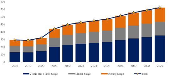
According to the new market research report “Global Precision Positioning Equipment Market Report 2023-2029”, published by QYResearch, the global Precision Positioning Equipment market size is projected to reach USD 0.72 billion by 2029, at a CAGR of 5.4% during the forecast period.

Figure. Global Precision Positioning Equipment Market Size (US$ Million), 2018-2029

Based on or includes research from QYResearch: Global Precision Positioning Equipment Market Report 2023-2029.
Market Drivers:
Increasing demand for smaller and more precise components has led to a focus on miniaturization and microfabrication. Precision positioning equipment is crucial for accurately manipulating tiny components and achieving high-resolution processing in various industries, including electronics and medical devices.
The semiconductor industry's continuous innovation and demand for higher processing power are driving the need for precision positioning equipment. Advancements in semiconductor manufacturing, including extreme ultraviolet (EUV) lithography and 3D packaging, rely on precise positioning solutions.
The growth of nanotechnology applications, such as nanomaterials and nanodevices, requires precise manipulation and positioning at the nanoscale. Precision positioning equipment plays a crucial role in enabling research and applications in this field.
Customers are increasingly seeking customized positioning solutions to meet specific requirements. Manufacturers are focusing on providing modular and flexible systems that can be tailored to various applications.
Restraint:
High Initial Costs: The upfront investment required for precision positioning equipment, including hardware, software, and installation, is significant. The semiconductor equipment industry is a typical technology-intensive and capital-intensive industry. The basic characteristics of this industry are high capital investment, long R&D cycle, strong technology, and high R&D risk.
Limited Affordability: Due to their advanced technology and high precision capabilities, precision positioning solutions may be out of reach for small and medium-sized enterprises (SMEs) and organizations with limited budgets.
Opportunity:
Complexity and Cost: Precision positioning equipment often involves advanced technologies and high-quality components, leading to higher manufacturing costs. The complexity of these systems can also lead to higher maintenance and operational costs.
High Precision Requirements: Meeting increasingly stringent precision requirements is a challenge. As industries demand submicron or even nanometer-level accuracy, designing, manufacturing, and calibrating equipment to consistently achieve such precision becomes more difficult.
Customization: Many companies require tailored solutions to suit their specific needs. Designing and manufacturing customized precision positioning equipment is challenging, as it requires expertise and resources to address unique requirements.
Figure. Global Precision Positioning Equipment Top 14 Players Ranking and Market Share(Continually updated)

Based on or includes research from QYResearch: Global Precision Positioning Equipment Market Report 2023-2029.
The global key manufacturers of Precision Positioning Equipment include Physik Instrumente (PI), Sumitomo Heavy Industries, NIPPON THOMPSON, SCHNEEBERGER, Aerotech, CKD NIKKI DENSO, Beijing U-PRECISION TECH, Kohzu Precision, HEPHAIST CO, Elliot Scientific, etc.
In 2022, the global top five players had a share approximately 30.0% in terms of revenue.
Figure. Precision Positioning Equipment, Global Market Size, Split by Product Segment
Based on or includes research from QYResearch: Global Precision Positioning Equipment Market Report 2023-2029.
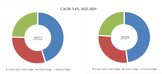
In terms of product type, currently 2-axis and 3-axis Stage is the largest segment, hold a share of 45.2%.
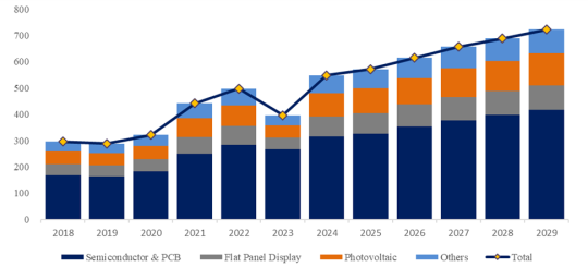
Figure. Precision Positioning Equipment, Global Market Size, Split by Application Segment

Based on or includes research from QYResearch: Global Precision Positioning Equipment Market Report 2023-2029.
In terms of product application, currently Semiconductor & PCB is the largest segment, hold a share of 57.3%.
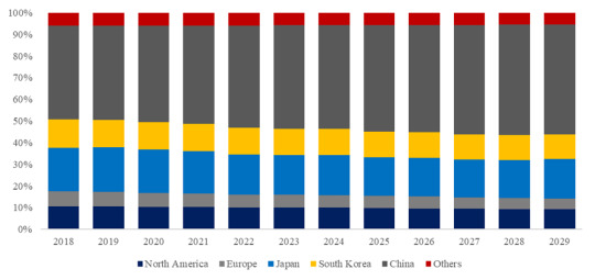
Figure. Precision Positioning Equipment, Global Market Size, Split by Region (Production)

Based on or includes research from QYResearch: Global Precision Positioning Equipment Market Report 2023-2029.
About The Authors
Yang Yang - Lead Author
Email: [email protected]
About QYResearch
QYResearch founded in California, USA in 2007.It is a leading global market research and consulting company. With over 16 years’ experience and professional research team in various cities over the world QY Research focuses on management consulting, database and seminar services, IPO consulting, industry chain research and customized research to help our clients in providing non-linear revenue model and make them successful. We are globally recognized for our expansive portfolio of services, good corporate citizenship, and our strong commitment to sustainability. Up to now, we have cooperated with more than 60,000 clients across five continents. Let’s work closely with you and build a bold and better future.
QYResearch is a world-renowned large-scale consulting company. The industry covers various high-tech industry chain market segments, spanning the semiconductor industry chain (semiconductor equipment and parts, semiconductor materials, ICs, Foundry, packaging and testing, discrete devices, sensors, optoelectronic devices), photovoltaic industry chain (equipment, cells, modules, auxiliary material brackets, inverters, power station terminals), new energy automobile industry chain (batteries and materials, auto parts, batteries, motors, electronic control, automotive semiconductors, etc.), communication industry chain (communication system equipment, terminal equipment, electronic components, RF front-end, optical modules, 4G/5G/6G, broadband, IoT, digital economy, AI), advanced materials industry Chain (metal materials, polymer materials, ceramic materials, nano materials, etc.), machinery manufacturing industry chain (CNC machine tools, construction machinery, electrical machinery, 3C automation, industrial robots, lasers, industrial control, drones), food, beverages and pharmaceuticals, medical equipment, agriculture, etc.
0 notes
Text
ASML의 EUV 장비, 한국에 생산 공장 설립 불가능한 이유
ASML의 EUV 장비, 한국에 생산 공장 설립 불가능한 이유
안녕하세요! 오늘은 ASML의 EUV 장비를 한국에 생산 공장을 설립하는 것이 왜 불가능한지에 대해 알아보겠습니다. ASML은 광학 및 반도체 산업에서 세계적인 기업으로, 그들의 EUV (Extreme Ultraviolet Lithography) 장비는 현대 반도체 제조에 중요한 역할을 합니다. 그러나 한국에서 이러한 장비를 생산하기 위해서는 다양한 이유로 높은 난이도와 도전이 있습니다. 이 글에서는 ASML의 EUV 장비를 한국에 생산하기 어려운 이유들을 자세히 살펴보겠습니다.
ASML: 세계적인 광학 및 반도체 기업
ASML은 네덜란드의 회사로서, 광학 및 반도체 산업에서 세계적인 지위를 차지하고 있습니다. 그들은 최신 기술과 혁신적인 아이디어로 많은 혁신을 이루어냈고, 특히 EUV 장비로 유명합니다.
EUV 국내 제조 공장 설립 가능성 '0%'
ASML의 EUV 장비를 한국에 생산하는 것은 현재로서는 '0%' 가능성이 있습니다. 경기도웨딩홀 이유에는 여러 가지 요소가 있는데, 주된 이유 중 하나는 기술력과 경쟁력의 부재입니다.
기술력 부재
한국은 반도체 제조 분야에서 많은 경쟁사들과 함께 성장해왔지만, ASML의 EUV 기술 수준에는 아직 도달하지 못했습니다. 이러한 고급 기술을 보유하고 있는 회사가 없기 때문에 한국에서 직접적으로 생산하는 것은 어려운 상황입니다.
경쟁력 부재
ASML은 전 세계적으로 막대한 시장 점유율을 보유하고 있으며, 다른 회사들이 그들과 경쟁하기 어려운 수준까지 도달했습니다. 한국 기업이 ASML과 경쟁하여 EUV 장비를 생산하는 것은 현재로서는 매우 어려운 일입니다.
ASML의 EUV 장비, 한국에 생산 공장 설립 불가능한 이유
ASML의 EUV 장비를 한국에 생산하는 것이 어렵다고 판단되는 주요 이유들을 정리해보겠습니다.
기술력 부재: ASML의 고급 기술 수준에 도달하지 못함.
경쟁력 부재: ASML과의 경쟁이 어려움.
시장 점유율: ASML이 이미 시장을 지배하고 있음.
자급자족 불가능: 필요한 자원과 인프라 구축이 어려움.
라이센스 문제: ASML의 특허와 라이센스 요건 충족 어려움.
글로벌 파트너십 필요: 글로벌 네트워크와 파트너십 필요성.
자주 묻는 질문 (FAQs)
ASML의 EUV 장비를 왜 한국에서 직접 생산하지 않는 걸까요?
한국의 기술력과 경쟁력 부재 때문입니다.
ASML의 EUV 장비를 구입하는 대신 왜 직접 생산하지 않나요?
ASML의 기술 수준과 시장 지배력으로 인해 어렵습니다.
한국에서도 같은 수준의 기술을 갖춘 회사가 없습니까?
아직까지 그런 회사가 없습니다.
ASML의 특허 문제로 인해 직접적인 생산이 어렵다고 들었습니다.
네, ASML은 자사 기술을 보호하기 위해 엄격한 특허 조건을 가지고 있습니다.
다른 국가에서는 생산되기 때문에 왜 한국만 안 되나요?
다른 국가들은 이미 필요한 인프라와 기반 시설 등을 보유했습니다.
앞으로 한국에서도 가능성이 있는 걸까요?
현재 상황에서는 어렵지만, 향후 발전 가능성은 항상 열려 있습니다.
결론
ASML의 EUV 장비를 한국에 직접적으로 생산하는 것은 현재로서는 많은 난관과 도전이 따르기 때문에 '0%' 가능성으로 평가됩니다. 하지만 지속적인 기술 발전과 노력으로 앞으로 가능성을 모색할 수 있을 것입니다.
감사합니다!
1 note
·
View note
Text
Semiconductor Manufacturing International Corp. has likely advanced its production technology by two generations, defying US sanctions intended to halt the rise of China’s largest chipmaker.
The Shanghai-based manufacturer is shipping Bitcoin-mining semiconductors built using 7-nanometer technology, industry watcher TechInsights wrote in a blog post on Tuesday. That’s well ahead of SMIC’s established 14nm technology, a measure of fabrication complexity in which narrower transistor widths help produce faster and more efficient chips. Since late 2020, the US has barred the unlicensed sale to the Chinese firm of equipment that can be used to fabricate semiconductors of 10nm and beyond, infuriating Beijing. [...]
A person familiar with the developments confirmed the report, asking not to be named as they were not authorized to discuss it publicly. SMIC climbed as much as 1.9% in Hong Kong, while Chinese chip and chip gear stocks including Shanghai Fudan Microelectronics Group Co., Naura Technology Group Co. and Advanced Micro-Fabrication Equipment Inc. gained more than 5%.[...]
SMIC’s surprising progress raises questions about how effective export controls have been and whether Washington can indeed thwart China’s ambition to foster a world-class chip industry at home and reduce reliance on foreign technologies. It also comes at a time American lawmakers have urged Washington to close loopholes in its Chinese-oriented curbs and ensure Beijing isn’t supplying crucial technology to Russia.[...]
SMIC has said that its blacklist status hurts its ability to develop sophisticated technologies. The company’s capability is severely curbed by its lack of access to ASML Holding NV’s extreme ultraviolet lithography (EUV) systems, which are required to make the most advanced chips that include 5nm and 3nm geometries. The Dutch firm has not shipped a single EUV machine to mainland China because of US pressure on the Dutch government.
21 Jul 22
45 notes
·
View notes
Text
ASML's High NA EUV Machine: Cutting edge semiconductor fabrication machine
Context: ASML’s new ‘High NA EUV’ machine, a groundbreaking semiconductor lithography device that costs $350 million and is crucial for creating the next generation of powerful computer chips. The machine uses extreme ultraviolet light and incredibly precise components to print intricate circuits on silicon wafers. It represents a significant technological advancement with strategic implications,…
View On WordPress
0 notes
Last Seen Blogs

thonikholis
Thoni Kholis

malecardiolove
Male Heart stories


fomybeloved
When You Know You Know

cantwaittomissthatone
Rouén D. E. Robinson