#Journal Progress in Photovoltaics
Text
Most work is new work, long-term study of U.S. census data shows
New Post has been published on https://sunalei.org/news/most-work-is-new-work-long-term-study-of-u-s-census-data-shows/
Most work is new work, long-term study of U.S. census data shows

This is part 1 of a two-part MIT News feature examining new job creation in the U.S. since 1940, based on new research from Ford Professor of Economics David Autor. Part 2 is available here.
In 1900, Orville and Wilbur Wright listed their occupations as “Merchant, bicycle” on the U.S. census form. Three years later, they made their famous first airplane flight in Kitty Hawk, North Carolina. So, on the next U.S. census, in 1910, the brothers each called themselves “Inventor, aeroplane.” There weren’t too many of those around at the time, however, and it wasn’t until 1950 that “Airplane designer” became a recognized census category.
Distinctive as their case may be, the story of the Wright brothers tells us something important about employment in the U.S. today. Most work in the U.S. is new work, as U.S. census forms reveal. That is, a majority of jobs are in occupations that have only emerged widely since 1940, according to a major new study of U.S. jobs led by MIT economist David Autor.
“We estimate that about six out of 10 jobs people are doing at present didn’t exist in 1940,” says Autor, co-author of a newly published paper detailing the results. “A lot of the things that we do today, no one was doing at that point. Most contemporary jobs require expertise that didn’t exist back then, and was not relevant at that time.”
This finding, covering the period 1940 to 2018, yields some larger implications. For one thing, many new jobs are created by technology. But not all: Some come from consumer demand, such as health care services jobs for an aging population.
On another front, the research shows a notable divide in recent new-job creation: During the first 40 years of the 1940-2018 period, many new jobs were middle-class manufacturing and clerical jobs, but in the last 40 years, new job creation often involves either highly paid professional work or lower-wage service work.
Finally, the study brings novel data to a tricky question: To what extent does technology create new jobs, and to what extent does it replace jobs?
The paper, “New Frontiers: The Origins and Content of New Work, 1940-2018,” appears in the Quarterly Journal of Economics. The co-authors are Autor, the Ford Professor of Economics at MIT; Caroline Chin, a PhD student in economics at MIT; Anna Salomons, a professor in the School of Economics at Utrecht University; and Bryan Seegmiller SM ’20, PhD ’22, an assistant professor at the Kellogg School of Northwestern University.
“This is the hardest, most in-depth project I’ve ever done in my research career,” Autor adds. “I feel we’ve made progress on things we didn’t know we could make progress on.”
“Technician, fingernail”
To conduct the study, the scholars dug deeply into government data about jobs and patents, using natural language processing techniques that identified related descriptions in patent and census data to link innovations and subsequent job creation. The U.S. Census Bureau tracks the emerging job descriptions that respondents provide — like the ones the Wright brothers wrote down. Each decade’s jobs index lists about 35,000 occupations and 15,000 specialized variants of them.
Many new occupations are straightforwardly the result of new technologies creating new forms of work. For instance, “Engineers of computer applications” was first codified in 1970, “Circuit layout designers” in 1990, and “Solar photovoltaic electrician” made its debut in 2018.
“Many, many forms of expertise are really specific to a technology or a service,” Autor says. “This is quantitatively a big deal.”
He adds: “When we rebuild the electrical grid, we’re going to create new occupations — not just electricians, but the solar equivalent, i.e., solar electricians. Eventually that becomes a specialty. The first objective of our study is to measure [this kind of process]; the second is to show what it responds to and how it occurs; and the third is to show what effect automation has on employment.”
On the second point, however, innovations are not the only way new jobs emerge. The wants and needs of consumers also generate new vocations. As the paper notes, “Tattooers” became a U.S. census job category in 1950, “Hypnotherapists” was codified in 1980, and “Conference planners” in 1990. Also, the date of U.S. Census Bureau codification is not the first time anyone worked in those roles; it is the point at which enough people had those jobs that the bureau recognized the work as a substantial employment category. For instance, “Technician, fingernail” became a category in 2000.
“It’s not just technology that creates new work, it’s new demand,” Autor says. An aging population of baby boomers may be creating new roles for personal health care aides that are only now emerging as plausible job categories.
All told, among “professionals,” essentially specialized white-collar workers, about 74 percent of jobs in the area have been created since 1940. In the category of “health services” — the personal service side of health care, including general health aides, occupational therapy aides, and more — about 85 percent of jobs have emerged in the same time. By contrast, in the realm of manufacturing, that figure is just 46 percent.
Differences by degree
The fact that some areas of employment feature relatively more new jobs than others is one of the major features of the U.S. jobs landscape over the last 80 years. And one of the most striking things about that time period, in terms of jobs, is that it consists of two fairly distinct 40-year periods.
In the first 40 years, from 1940 to about 1980, the U.S. became a singular postwar manufacturing powerhouse, production jobs grew, and middle-income clerical and other office jobs grew up around those industries.
But in the last four decades, manufacturing started receding in the U.S., and automation started eliminating clerical work. From 1980 to the present, there have been two major tracks for new jobs: high-end and specialized professional work, and lower-paying service-sector jobs, of many types. As the authors write in the paper, the U.S. has seen an “overall polarization of occupational structure.”
That corresponds with levels of education. The study finds that employees with at least some college experience are about 25 percent more likely to be working in new occupations than those who possess less than a high school diploma.
“The real concern is for whom the new work has been created,” Autor says. “In the first period, from 1940 to 1980, there’s a lot of work being created for people without college degrees, a lot of clerical work and production work, middle-skill work. In the latter period, it’s bifurcated, with new work for college graduates being more and more in the professions, and new work for noncollege graduates being more and more in services.”
Still, Autor adds, “This could change a lot. We’re in a period of potentially consequential technology transition.”
At the moment, it remains unclear how, and to what extent, evolving technologies such as artificial intelligence will affect the workplace. However, this is also a major issue addressed in the current research study: How much does new technology augment employment, by creating new work and viable jobs, and how much does new technology replace existing jobs, through automation? In their paper, Autor and his colleagues have produced new findings on that topic, which are outlined in part 2 of this MIT News series.
Support for the research was provided, in part, by the Carnegie Corporation; Google; Instituut Gak; the MIT Work of the Future Task Force; Schmidt Futures; the Smith Richardson Foundation; and the Washington Center for Equitable Growth.
0 notes
Text
Most work is new work, long-term study of U.S. census data shows
New Post has been published on https://thedigitalinsider.com/most-work-is-new-work-long-term-study-of-u-s-census-data-shows/
Most work is new work, long-term study of U.S. census data shows

This is part 1 of a two-part MIT News feature examining new job creation in the U.S. since 1940, based on new research from Ford Professor of Economics David Autor. Part 2 is available here.
In 1900, Orville and Wilbur Wright listed their occupations as “Merchant, bicycle” on the U.S. census form. Three years later, they made their famous first airplane flight in Kitty Hawk, North Carolina. So, on the next U.S. census, in 1910, the brothers each called themselves “Inventor, aeroplane.” There weren’t too many of those around at the time, however, and it wasn’t until 1950 that “Airplane designer” became a recognized census category.
Distinctive as their case may be, the story of the Wright brothers tells us something important about employment in the U.S. today. Most work in the U.S. is new work, as U.S. census forms reveal. That is, a majority of jobs are in occupations that have only emerged widely since 1940, according to a major new study of U.S. jobs led by MIT economist David Autor.
“We estimate that about six out of 10 jobs people are doing at present didn’t exist in 1940,” says Autor, co-author of a newly published paper detailing the results. “A lot of the things that we do today, no one was doing at that point. Most contemporary jobs require expertise that didn’t exist back then, and was not relevant at that time.”
This finding, covering the period 1940 to 2018, yields some larger implications. For one thing, many new jobs are created by technology. But not all: Some come from consumer demand, such as health care services jobs for an aging population.
On another front, the research shows a notable divide in recent new-job creation: During the first 40 years of the 1940-2018 period, many new jobs were middle-class manufacturing and clerical jobs, but in the last 40 years, new job creation often involves either highly paid professional work or lower-wage service work.
Finally, the study brings novel data to a tricky question: To what extent does technology create new jobs, and to what extent does it replace jobs?
The paper, “New Frontiers: The Origins and Content of New Work, 1940-2018,” appears in the Quarterly Journal of Economics. The co-authors are Autor, the Ford Professor of Economics at MIT; Caroline Chin, a PhD student in economics at MIT; Anna Salomons, a professor in the School of Economics at Utrecht University; and Bryan Seegmiller SM ’20, PhD ’22, an assistant professor at the Kellogg School of Northwestern University.
“This is the hardest, most in-depth project I’ve ever done in my research career,” Autor adds. “I feel we’ve made progress on things we didn’t know we could make progress on.”
“Technician, fingernail”
To conduct the study, the scholars dug deeply into government data about jobs and patents, using natural language processing techniques that identified related descriptions in patent and census data to link innovations and subsequent job creation. The U.S. Census Bureau tracks the emerging job descriptions that respondents provide — like the ones the Wright brothers wrote down. Each decade’s jobs index lists about 35,000 occupations and 15,000 specialized variants of them.
Many new occupations are straightforwardly the result of new technologies creating new forms of work. For instance, “Engineers of computer applications” was first codified in 1970, “Circuit layout designers” in 1990, and “Solar photovoltaic electrician” made its debut in 2018.
“Many, many forms of expertise are really specific to a technology or a service,” Autor says. “This is quantitatively a big deal.”
He adds: “When we rebuild the electrical grid, we’re going to create new occupations — not just electricians, but the solar equivalent, i.e., solar electricians. Eventually that becomes a specialty. The first objective of our study is to measure [this kind of process]; the second is to show what it responds to and how it occurs; and the third is to show what effect automation has on employment.”
On the second point, however, innovations are not the only way new jobs emerge. The wants and needs of consumers also generate new vocations. As the paper notes, “Tattooers” became a U.S. census job category in 1950, “Hypnotherapists” was codified in 1980, and “Conference planners” in 1990. Also, the date of U.S. Census Bureau codification is not the first time anyone worked in those roles; it is the point at which enough people had those jobs that the bureau recognized the work as a substantial employment category. For instance, “Technician, fingernail” became a category in 2000.
“It’s not just technology that creates new work, it’s new demand,” Autor says. An aging population of baby boomers may be creating new roles for personal health care aides that are only now emerging as plausible job categories.
All told, among “professionals,” essentially specialized white-collar workers, about 74 percent of jobs in the area have been created since 1940. In the category of “health services” — the personal service side of health care, including general health aides, occupational therapy aides, and more — about 85 percent of jobs have emerged in the same time. By contrast, in the realm of manufacturing, that figure is just 46 percent.
Differences by degree
The fact that some areas of employment feature relatively more new jobs than others is one of the major features of the U.S. jobs landscape over the last 80 years. And one of the most striking things about that time period, in terms of jobs, is that it consists of two fairly distinct 40-year periods.
In the first 40 years, from 1940 to about 1980, the U.S. became a singular postwar manufacturing powerhouse, production jobs grew, and middle-income clerical and other office jobs grew up around those industries.
But in the last four decades, manufacturing started receding in the U.S., and automation started eliminating clerical work. From 1980 to the present, there have been two major tracks for new jobs: high-end and specialized professional work, and lower-paying service-sector jobs, of many types. As the authors write in the paper, the U.S. has seen an “overall polarization of occupational structure.”
That corresponds with levels of education. The study finds that employees with at least some college experience are about 25 percent more likely to be working in new occupations than those who possess less than a high school diploma.
“The real concern is for whom the new work has been created,” Autor says. “In the first period, from 1940 to 1980, there’s a lot of work being created for people without college degrees, a lot of clerical work and production work, middle-skill work. In the latter period, it’s bifurcated, with new work for college graduates being more and more in the professions, and new work for noncollege graduates being more and more in services.”
Still, Autor adds, “This could change a lot. We’re in a period of potentially consequential technology transition.”
At the moment, it remains unclear how, and to what extent, evolving technologies such as artificial intelligence will affect the workplace. However, this is also a major issue addressed in the current research study: How much does new technology augment employment, by creating new work and viable jobs, and how much does new technology replace existing jobs, through automation? In their paper, Autor and his colleagues have produced new findings on that topic, which are outlined in part 2 of this MIT News series.
Support for the research was provided, in part, by the Carnegie Corporation; Google; Instituut Gak; the MIT Work of the Future Task Force; Schmidt Futures; the Smith Richardson Foundation; and the Washington Center for Equitable Growth.
#000#aging#applications#artificial#Artificial Intelligence#automation#baby#career#change#college#computer#conference#consumers#content#data#deal#designers#Economics#education#electrical grid#employees#employment#engineers#Features#flight#Ford#form#Forms#Foundation#Future
0 notes
Text
Ethylene Vinyl Acetate Market 2023 – Competitive Approach, Fundamental Trends and Investment up to 2032
A complete overview of the market, including different aspects of market analysis, product definition, market segmentation, significant developments, and the current vendor landscape, is presented in the Ethylene Vinyl Acetate Market report. This market research report analyses the market structure in great detail and rates the major market segments and sub-segments. For the purpose of putting together the data and information mentioned in this market report, a variety of reliable sources were used, including journals, websites, annual reports of the companies, white papers, and mergers. The customer can better understand the various market drivers and restraints by using the results of the Ethylene Vinyl Acetate Market research study.
Download FREE Sample Copy of This Report:
Ethylene Vinyl Acetate Market analysis report has been mainly designed by keeping in mind the customer requirements which will ultimately assist them in boosting their return on investment (ROI). Furthermore, this research report takes into consideration several industry verticals such as company profile, contact details of manufacturer product specifications, geographical scope, production value, market structures, recent developments, revenue analysis, market shares, and possible sales volume of the company. The data, information, statistics, facts, and figures covered in the report lend a hand to the industry in maximizing or minimizing the offerings depending on the conditions of demand.
Competitive Landscape
The global market for EVA is highly consolidated with only a few tier-1 manufacturers occupying a large share of the market. The focus of major players across the world is mostly on product development and distribution network expansion.
Prominent players in the market follow the competitive market pricing strategy in the ethylene vinyl acetate market. Companies are entering into collaborations and partnerships with end-use industries to bolster their consumer base.
ExxonMobil Corporation, in 2019, acquired Materia, Inc. The high structural performance company is a Nobel prize-winning firm for the technology for manufacturing a new class of materials.
Celanese Corporation, in 2019, announced the acquisition of Next Polymers Ltd. This acquisition is likely to lead to rapid growth in the Indian business and broaden the company’s ability to serve nylon and other engineered materials coupled with offering a wide range of polymer products over the coming years
Ethylene Vinyl Acetate Industry Research by Category
Ethylene Vinyl Acetate Market by Product Type :
Very Low Density EVA
Low Density EVA
Medium Density EVA
High Density EVA
Ethylene Vinyl Acetate Market by End-use Industry :
Footwear & Foam
Packaging
Agriculture
Photovoltaic Panels
Pharmaceuticals
Other End-use Industries
Ethylene Vinyl Acetate Market by Region :
North America
Latin America
Europe
APAC
MEA
What insights readers can gather from the Ethylene Vinyl Acetate Market report?
A critical study of the Ethylene Vinyl Acetate Market on the basis of segment 1, segment 2 and segment 3.
Learn the behavior pattern of every Ethylene Vinyl Acetate Market player – product launches, expansions, collaborations and acquisitions in the market currently.
Examine and study the progress outlook of the global Ethylene Vinyl Acetate Market landscape, which includes, revenue, production & consumption and historical & forecast.
Understand important drivers, restraints, opportunities, and trends (DROT Analysis).
Important trends, such as carbon footprint, R&D developments, prototype technologies, and globalization.
The Ethylene Vinyl Acetate Market report will improve the revenue impact of businesses in various industries by:
Providing a framework tailored toward understanding the attractiveness quotient of various products/solutions/technologies in the Ethylene Vinyl Acetate Market
Guiding stakeholders to identify key problem areas pertaining to their consolidation strategies in the global Ethylene Vinyl Acetate Market and offers solutions
Assessing the impact of changing regulatory dynamics in the regions in which companies are keen on expanding their footprints
Provides understanding of disruptive technology trends to help businesses make their transitions smoothly
Helping leading companies make strategy recalibrations ahead of their competitors and peers
Offers insights into promising synergies for top players aiming to retain their leadership position in the Ethylene Vinyl Acetate Market.
0 notes
Text
Upconversion Particles’ Role in Composite Materials: From Light Absorption to Energy Conversion_Crimson Publishers

Upconversion Particles’ Role in Composite Materials: From Light Absorption to Energy Conversion by Bastani S* in Crimson Publishers: Peer Reviewed Material Science Journals
Upconversion materials are capable of emitting high-energy photons in the span of ultraviolet to NIR region of electromagnetic spectrum under excitation by low energy NIR photons through a process termed ‘upconversion fluorescence’. The NIR electromagnetic wave has deeper penetration, lower thermal effect, and lower toxicity compared with UV/vis laser, providing UC materials with a wide range of applications. This review focuses on the research progress of the application of UC particles and their role in composite materials, which covers the field of radiation curing technology, anti-counterfeiting technology, photovoltaics, and photocatalysis.
For more Open access journals in Crimson Publishers please click on below link https://crimsonpublishersresearch.com/
For more article in Peer Reviewed Material Science Journals please click on below link https://crimsonpublishers.com/rdms/
#crimson publishers#Crimson Publishers LLC#Upconversion particles#Light absorption#Energy conversion
0 notes
Text
Australian researchers show next gen solar cells can beat the heat
Australian researchers show next gen solar cells can beat the heat
Good News Notes:
“Australian researchers have demonstrated that new solar panel designs and manufacturing techniques have the potential to solve some of the key challenges of operating in high temperatures, showing that they not only produce more useful electricity but have longer operational lives thanks to their ability to beat the heat.
In new research published in the journal Progress in…

View On WordPress
#ARC Centre of Excellence in Exciton Science#Australia#computer processors#electron#good news#happy#heat-related degradation#help#higher efficiencies#Journal Progress in Photovoltaics#joy#kindness#lower operating temperatures#manufacturing techniques#more electricity#need#new research#perovskite#photon#positive#renewable energy#researchers#School of Photovoltaic and Renewable Energy Engineering#silicon cells#singlet fission#solar energy#solar panel#sunlight#tandem solar cells#temperature
13 notes
·
View notes
Photo

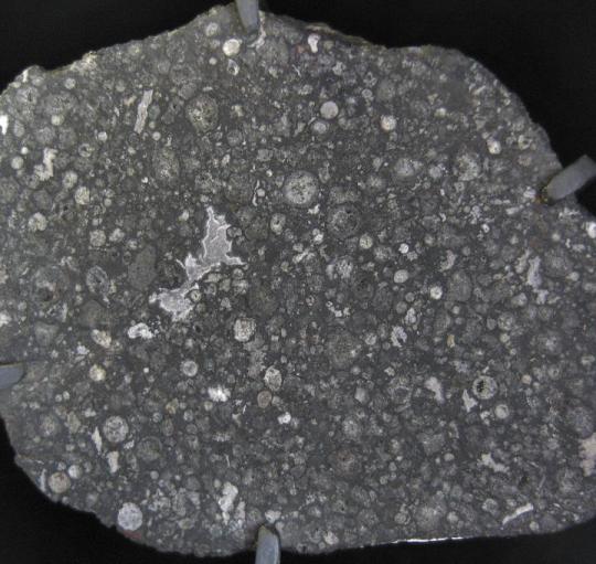
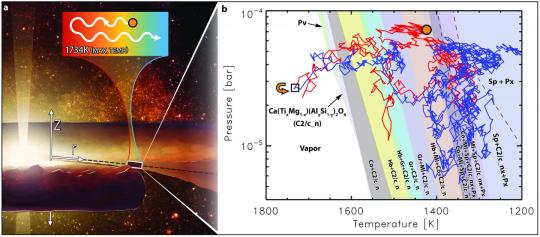
Researchers trace dust grain's journey through newborn solar system A research team led by the University of Arizona has reconstructed in unprecedented detail the history of a dust grain that formed during the birth of the solar system more than 4.5 billion years ago. The findings provide insights into the fundamental processes underlying the formation of planetary systems, many of which are still shrouded in mystery. For the study, the team developed a new type of framework, which combines quantum mechanics and thermodynamics, to simulate the conditions to which the grain was exposed during its formation, when the solar system was a swirling disk of gas and dust known as a protoplanetary disk or solar nebula. Comparing the predictions from the model to an extremely detailed analysis of the sample's chemical makeup and crystal structure, along with a model of how matter was transported in the solar nebula, revealed clues about the grain's journey and the environmental conditions that shaped it along the way. The grain analyzed in the study is one of several inclusions, known as calcium-aluminum rich inclusions, or CAIs, discovered in a sample from the Allende meteorite, which fell over the Mexican state of Chihuahua in 1969. CAIs are of special interest because they are thought to be among the first solids that formed in the solar system more than 4.5 billion years ago. Similar to how stamps in a passport tell a story about a traveler's journey and stops along the way, the samples' micro- and atomic-scale structures unlock a record of their formation histories, which were controlled by the collective environments to which they were exposed. "As far as we know, our paper is the first to tell an origin story that offers clues about the likely processes that happened at the scale of astronomical distances with what we see in our sample at the scale of atomic distances," said Tom Zega, a professor in the University of Arizona's Lunar and Planetary Laboratory and the first author of the paper, published in The Planetary Science Journal. Zega and his team analyzed the composition of the inclusions embedded in the meteorite using cutting-edge atomic-resolution scanning transmission electron microscopes - one at UArizona's Kuiper Materials Imaging and Characterization Facility, and its sister microscope located at the Hitachi factory in Hitachinaka, Japan. The inclusions were found to consist mainly of types of minerals known as spinel and perovskite, which also occur in rocks on Earth and are being studied as candidate materials for applications such as microelectronics and photovoltaics. Similar kinds of solids occur in other types of meteorites known as carbonaceous chondrites, which are particularly interesting to planetary scientists as they are known to be leftovers from the formation of the solar system and contain organic molecules, including those that may have provided the raw materials for life. Precisely analyzing the spatial arrangement of atoms allowed the team to study the makeup of the underlying crystal structures in great detail. To the team's surprise, some of the results were at odds with current theories on the physical processes thought to be active inside protoplanetary disks, prompting them to dig deeper. "Our challenge is that we don't know what chemical pathways led to the origins of these inclusions," Zega said. "Nature is our lab beaker, and that experiment took place billions of years before we existed, in a completely alien environment." Zega said the team set out to "reverse-engineer" the makeup of the extraterrestrial samples by designing new models that simulated complex chemical processes, which the samples would be subjected to inside a protoplanetary disk. "Such models require an intimate convergence of expertise spanning the fields of planetary science, materials science, mineral science and microscopy, which was what we set out to do," added Krishna Muralidharan, a study co-author and an associate professor in the UArizona's Department of Materials Science and Engineering. Based on the data the authors were able to tease from their samples, they concluded that the particle formed in a region of the protoplanetary disk not far from where Earth is now, then made a journey closer to the sun, where it was progressively hotter, only to later reverse course and wash up in cooler parts farther from the young sun. Eventually, it was incorporated into an asteroid, which later broke apart into pieces. Some of those pieces were captured by Earth's gravity and fell as meteorites. The samples for this study were taken from the inside of a meteorite and are considered primitive - in other words, unaffected by environmental influences. Such primitive material is believed to not have undergone any significant changes since it first formed more than 4.5 billion years ago, which is rare. Whether similar objects occur in asteroid Bennu, samples of which will be returned to Earth by the UArizona-led OSIRIS-REx mission in 2023, remains to be seen. Until then, scientists rely on samples that fall to Earth via meteorites. "This material is our only record of what happened 4.567 billion years ago in the solar nebula," said Venkat Manga, a co-author of the paper and an assistant research professor in the UArizona Department of Materials Science and Engineering. "Being able to look at the microstructure of our sample at different scales, down to the length of individual atoms, is like opening a book." The authors said that studies like this one could bring planetary scientists a step closer to "a grand model of planet formation" - a detailed understanding of the material moving around the disk, what it is composed of, and how it gives rise to the sun and the planets. Powerful radio telescopes like the Atacama Large Millimeter/submillimeter Array, or ALMA, in Chile now allow astronomers to see stellar systems as they evolve, Zega said. "Perhaps at some point we can peer into evolving disks, and then we can really compare our data between disciplines and begin answering some of those really big questions," Zega said. "Are these dust particles forming where we think they did in our own solar system? Are they common to all stellar systems? Should we expect the pattern we see in our solar system - rocky planets close to the central star and gas giants farther out - in all systems? "It's a really interesting time to be a scientist when these fields are evolving so rapidly," he added. "And it's awesome to be at an institution where researchers can form transdisciplinary collaborations among leading astronomy, planetary and materials science departments at the same university." TOP IMAGE....Artist's illustration of the early solar system, at a time when no planets had formed yet. A swirling cloud of gas and dust surrounded the young sun. The cutaway through this so-called protoplanetary disk shows its three-dimensional structure. CREDIT Heather Roper CENTRE IMAGE....A slice through an Allende meteorite reveals various spherical particles, known as chondrules. The irregularly shaped "island" left of the center is a calcium-aluminum rich inclusion, or CAI. The grain in this study was isolated from such a CAI. CREDIT Shiny Things/Wikimedia Commons LOWER IMAGE....Illustration of the dynamic history that the modeled particle could have experienced during the formation of the solar system. Analyzing the particle's micro- and atomic-scale structures and combining them with new models that simulated complex chemical processes in the disk revealed its possible journey over the course of many orbits around the sun (callout box and diagram on the right). Originating not far from where Earth would form, the grain was transported into the inner, hotter regions, and eventually washed up in cooler regions. CREDIT Heather Roper/Tom Zega et al.
6 notes
·
View notes
Text
Breakthrough in new material to harness solar power
The most affordable, efficient way to harness the cleanest, most abundant renewable energy source in the world is one step closer to reality.

The University of Toledo physicist pushing the performance of solar cells to levels never before reached made a significant breakthrough in the chemical formula and process to make the new material.
Working in collaboration with the U.S. Department of Energy's National Renewable Energy Lab and the University of Colorado, Dr. Yanfa Yan, UToledo professor of physics, envisions the ultra-high efficiency material called a tandem perovskite solar cell will be ready to debut in full-sized solar panels in the consumer market in the near future.
Perovskites, compound materials with a special crystal structure formed through chemistry, would replace silicon, which -- for now -- remains the solar-cell material of choice for converting the sun's light into electrical energy.
"We are producing higher-efficiency, lower-cost solar cells that show great promise to help solve the world energy crisis," Yan said. "The meaningful work will help protect our planet for our children and future generations. We have a problem consuming most of the fossil energies right now, and our collaborative team is focused on refining our innovative way to clean up the mess."
The new research paper, which is published in the journal Science, outlines how the photovoltaics team is fine-tuning a mix of lead and tin to advance the technology closer to its maximum efficiency. Efforts have currently brought the efficiency of the new solar cell to about 23 percent. In comparison, silicon solar panels on the market today have around an 18 percent efficiency rating.
Scientists used a chemical compound called guanidinium thiocyanate to dramatically improve the structural and optoelectronic properties of the lead-tin mixed perovskite films.
"Science is the top academic journal in the world, alongside Nature, which published other research by Dr. Yan only five months ago after he discovered a single material that produces white light, which could boost the efficiency and appeal of LED bulbs," Dr. Sanjay Khare, professor and chair of the UToledo Department of Physics and Astronomy, said. "His significant sustainability work at The University of Toledo can help power the world using clean energy."
About five years ago Yan's team at UToledo identified the ideal properties of perovskites and he has since focused his 20 years of experience on producing an all-perovskite tandem solar cell that brings together two different solar cells to increase the total electrical power generated by using two different parts of the sun's spectrum.
Last month the U.S. Department of Energy awarded Yan a $1.1 million grant to continue his research in collaboration with the National Renewable Energy Lab.
"This is the material we've been waiting for for a long time," Yan said. "The solar industry is watching and waiting. Some have already started investing in this technology."
Yan is an expert in theory of defect physics and electronic properties in semiconductors, materials synthesis and thin-film solar-cell fabrication.
"Our UToledo research is ongoing to make cheaper and more efficient solar cells that could rival and even outperform the prevailing silicon photovoltaic technology," said Dr. Zhaoning Song, research assistant professor in the UToledo Department of Physics and Astronomy and co-author on the study. "Our tandem solar cells with two layers of perovskites deliver high power conversion efficiency and have the potential to bring down production costs of solar panels, which is an important advance in photovoltaics."
While Yan's team has improved the quality of the materials and the process to manufacture them at a low cost, more progress needs to be made.
"The material cost is low and the fabrication cost is low, but the lifetime of the material is still an unknown," Song said. "We need to continue to increase efficiency and stability."
"Also, lead is considered a toxic substance," Yan said. "I am determined to work with the solar industry to ensure solar panels made of this material can be recycled so they don't cause harm to the environment."
119 notes
·
View notes
Photo

The Graphene Based Materials Used in Energy
by Tarun Radadiya "The Graphene Based Materials Used in Energy"
Published in International Journal of Trend in Scientific Research and Development (ijtsrd), ISSN: 2456-6470, Volume-5 | Issue-4 , June 2021,
URL: https://www.ijtsrd.compapers/ijtsrd42512.pdf
Paper URL: https://www.ijtsrd.comother-scientific-research-area/other/42512/the-graphene-based-materials-used-in-energy/tarun-radadiya
callforpaperbiologicalscience, biologicalsciencejournal
Graphene two dimensional carbon sheet with one atom thickness and one of the thinnest materials in universe. However, pure Graphene sheets are limited for many applications despite their excellent characteristics and scientists face challenges to induce more and controlled functionality. The nanomaterials inherit the unique properties of Graphene, and the addition of functional groups or the nanoparticle composites on their surfaces improves their performance. Therefore Graphene nanocomposites or hybrids are attracting increasing efforts for real applications in energy and environmental areas by introducing controlled functional building blocks to Graphene. Nanocomposites energy related progress of Graphene nanocomposites in solar energy conversion e.g., photovoltaic and photo electrochemical devices, artificial photosynthesis and electrochemical energy devices e.g., lithium ion battery, super capacitor, fuel cell . The Graphene nanocomposites advances in environmental applications of functionalized Graphene nanocomposites for the detection and removal of heavy metal ions, organic pollutants, gas and bacteria, treatment of environmental pollution, environmental protection and detection. Graphene nanocomposites in energy and environmental science.
0 notes
Text
I Found This Interesting. Joshua Damien Cordle
On the road to invisible solar panels: How tomorrow's windows will generate electricity
Five years after the Paris climate agreement, all eyes are on the world's progress on the road to a carbon-free future. A crucial part of this goal involves the energy transition from fossil fuels to renewable sources, such as sun, water, wind and wave energy. Among those, solar energy has always held the highest hope in the scientific community, as the most reliable and abundant energy source on Earth. In recent decades, solar cells have become cheaper, more efficient, and environment friendly. However, current solar cells tend to be opaque, which prevents their wider use and integration into everyday materials, constrained to being lined up on roofs and in remote solar farms.
But what if next-generation solar panels could be integrated to windows, buildings, or even mobile phone screens? That is the hope of Professor Joondong Kim from the Department of Electrical Engineering at Incheon National University, Korea. In a recent study published in Journal of Power Sources, he and his colleagues detail their latest invention: a fully transparent solar cell. "The unique features of transparent photovoltaic cells could have various applications in human technology," says Prof. Kim.
The idea of transparent solar cells is well known, but this novel application where scientists have been able to translate this idea into practice is a crucial new finding. At present, the materials making the solar cell opaque are the semiconductor layers, those responsible for capturing light and translating it into an electrical current. Hence, Prof. Kim and his colleagues looked at two potential semiconductor materials, identified by previous researchers for their desirable properties.
The first is titanium dioxide (TiO2), a well-known semiconductor already widely used to make solar cells. On top of its excellent electrical properties, TiO2 is also an environment-friendly and non-toxic material. This material absorbs UV light (a part of the light spectrum invisible to the naked eye) while letting through most of the visible light range. The second material investigated to make this junction was nickel oxide (NiO), another semiconductor known to have high optical transparency. As nickel is one of the mist abundant elements on Earth, and its oxide can easily be manufactured at low industrial temperatures, NiO is also a great material to make eco-friendly cells.
The solar cell prepared by the researchers was composed of a glass substrate and a metal oxide electrode, on top of which they deposited thin layers of the semiconductors (TiO2 first, then NiO) and a final coating of silver nanowires, acting as the other electrode in the cell. They ran several tests to evaluate the device's absorbance and transmittance of light, as well as its effectiveness as a solar cell.
Their findings were encouraging; with a power conversion efficiency of 2.1%, the cell's performance was quite good, given that it targets only a small part of the light spectrum. The cell was also highly responsive and worked in low light conditions. Furthermore, more than 57% of visible light was transmitted through the cell's layers, giving the cell this transparent aspect. In the final part of their experiment, the researchers demonstrated how their device could be used to power a small motor. "While this innovative solar cell is still very much in its infancy, our results strongly suggest that further improvement is possible for transparent photovoltaics by optimizing the cell's optical and electrical properties," suggests Prof. Kim.
Now that they have demonstrated the practicality of a transparent solar cell, they hope to further improve its efficiency in the near future. Only further research can tell whether they will indeed become a reality, but for all intents and purposes, this new technology opens a -- quite literal -- window into the future of clean energy.
Story Source:
Materials provided by Incheon National University. Note: Content may be edited for style and length.
Journal Reference:
Thanh Tai Nguyen, Malkeshkumar Patel, Sangho Kim, Rameez Ahmad Mir, Junsin Yi, Vinh-Ai Dao, Joondong Kim. Transparent photovoltaic cells and self-powered photodetectors by TiO2/NiO heterojunction. Journal of Power Sources, 2021; 481: 228865 DOI: 10.1016/j.jpowsour.2020.228865
0 notes
Text
Study unlocks nanoscale secrets for designing next-generation solar cells
New Post has been published on https://sunalei.org/news/study-unlocks-nanoscale-secrets-for-designing-next-generation-solar-cells/
Study unlocks nanoscale secrets for designing next-generation solar cells

Perovskites, a broad class of compounds with a particular kind of crystal structure, have long been seen as a promising alternative or supplement to today’s silicon or cadmium telluride solar panels. They could be far more lightweight and inexpensive, and could be coated onto virtually any substrate, including paper or flexible plastic that could be rolled up for easy transport.
In their efficiency at converting sunlight to electricity, perovskites are becoming comparable to silicon, whose manufacture still requires long, complex, and energy-intensive processes. One big remaining drawback is longevity: They tend to break down in a matter of months to years, while silicon solar panels can last more than two decades. And their efficiency over large module areas still lags behind silicon. Now, a team of researchers at MIT and several other institutions has revealed ways to optimize efficiency and better control degradation, by engineering the nanoscale structure of perovskite devices.
The study reveals new insights on how to make high-efficiency perovskite solar cells, and also provides new directions for engineers working to bring these solar cells to the commercial marketplace. The work is described today in the journal Nature Energy, in a paper by Dane deQuilettes, a recent MIT postdoc who is now co-founder and chief science officer of the MIT spinout Optigon, along with MIT professors Vladimir Bulovic and Moungi Bawendi, and 10 others at MIT and in Washington state, the U.K., and Korea.
“Ten years ago, if you had asked us what would be the ultimate solution to the rapid development of solar technologies, the answer would have been something that works as well as silicon but whose manufacturing is much simpler,” Bulovic says. “And before we knew it, the field of perovskite photovoltaics appeared. They were as efficient as silicon, and they were as easy to paint on as it is to paint on a piece of paper. The result was tremendous excitement in the field.”
Nonetheless, “there are some significant technical challenges of handling and managing this material in ways we’ve never done before,” he says. But the promise is so great that many hundreds of researchers around the world have been working on this technology. The new study looks at a very small but key detail: how to “passivate” the material’s surface, changing its properties in such a way that the perovskite no longer degrades so rapidly or loses efficiency.
“The key is identifying the chemistry of the interfaces, the place where the perovskite meets other materials,” Bulovic says, referring to the places where different materials are stacked next to perovskite in order to facilitate the flow of current through the device.
Engineers have developed methods for passivation, for example by using a solution that creates a thin passivating coating. But they’ve lacked a detailed understanding of how this process works — which is essential to make further progress in finding better coatings. The new study “addressed the ability to passivate those interfaces and elucidate the physics and science behind why this passivation works as well as it does,” Bulovic says.
The team used some of the most powerful instruments available at laboratories around the world to observe the interfaces between the perovskite layer and other materials, and how they develop, in unprecedented detail. This close examination of the passivation coating process and its effects resulted in “the clearest roadmap as of yet of what we can do to fine-tune the energy alignment at the interfaces of perovskites and neighboring materials,” and thus improve their overall performance, Bulovic says.
While the bulk of a perovskite material is in the form of a perfectly ordered crystalline lattice of atoms, this order breaks down at the surface. There may be extra atoms sticking out or vacancies where atoms are missing, and these defects cause losses in the material’s efficiency. That’s where the need for passivation comes in.
“This paper is essentially revealing a guidebook for how to tune surfaces, where a lot of these defects are, to make sure that energy is not lost at surfaces,” deQuilettes says. “It’s a really big discovery for the field,” he says. “This is the first paper that demonstrates how to systematically control and engineer surface fields in perovskites.”
The common passivation method is to bathe the surface in a solution of a salt called hexylammonium bromide, a technique developed at MIT several years ago by Jason Jungwan Yoo PhD ’20, who is a co-author of this paper, that led to multiple new world-record efficiencies. By doing that “you form a very thin layer on top of your defective surface, and that thin layer actually passivates a lot of the defects really well,” deQuilettes says. “And then the bromine, which is part of the salt, actually penetrates into the three-dimensional layer in a controllable way.” That penetration helps to prevent electrons from losing energy to defects at the surface.
These two effects, produced by a single processing step, produces the two beneficial changes simultaneously. “It’s really beautiful because usually you need to do that in two steps,” deQuilettes says.
The passivation reduces the energy loss of electrons at the surface after they have been knocked loose by sunlight. These losses reduce the overall efficiency of the conversion of sunlight to electricity, so reducing the losses boosts the net efficiency of the cells.
That could rapidly lead to improvements in the materials’ efficiency in converting sunlight to electricity, he says. The recent efficiency records for a single perovskite layer, several of them set at MIT, have ranged from about 24 to 26 percent, while the maximum theoretical efficiency that could be reached is about 30 percent, according to deQuilettes.
An increase of a few percent may not sound like much, but in the solar photovoltaic industry such improvements are highly sought after. “In the silicon photovoltaic industry, if you’re gaining half of a percent in efficiency, that’s worth hundreds of millions of dollars on the global market,” he says. A recent shift in silicon cell design, essentially adding a thin passivating layer and changing the doping profile, provides an efficiency gain of about half of a percent. As a result, “the whole industry is shifting and rapidly trying to push to get there.” The overall efficiency of silicon solar cells has only seen very small incremental improvements for the last 30 years, he says.
The record efficiencies for perovskites have mostly been set in controlled laboratory settings with small postage-stamp-size samples of the material. “Translating a record efficiency to commercial scale takes a long time,” deQuilettes says. “Another big hope is that with this understanding, people will be able to better engineer large areas to have these passivating effects.”
There are hundreds of different kinds of passivating salts and many different kinds of perovskites, so the basic understanding of the passivation process provided by this new work could help guide researchers to find even better combinations of materials, the researchers suggest. “There are so many different ways you could engineer the materials,” he says.
“I think we are on the doorstep of the first practical demonstrations of perovskites in the commercial applications,” Bulovic says. “And those first applications will be a far cry from what we’ll be able to do a few years from now.” He adds that perovskites “should not be seen as a displacement of silicon photovoltaics. It should be seen as an augmentation — yet another way to bring about more rapid deployment of solar electricity.”
“A lot of progress has been made in the last two years on finding surface treatments that improve perovskite solar cells,” says Michael McGehee, a professor of chemical engineering at the University of Colorado who was not associated with this research. “A lot of the research has been empirical with the mechanisms behind the improvements not being fully understood. This detailed study shows that treatments can not only passivate defects, but can also create a surface field that repels carriers that should be collected at the other side of the device. This understanding might help further improve the interfaces.”
The team included researchers at the Korea Research Institute of Chemical Technology, Cambridge University, the University of Washington in Seattle, and Sungkyunkwan University in Korea. The work was supported by the Tata Trust, the MIT Institute for Soldier Nanotechnologies, the U.S. Department of Energy, and the U.S. National Science Foundation.
1 note
·
View note
Text
Study Unlocks Nanoscale Secrets for Designing Next-Generation Solar Cells - Technology Org
New Post has been published on https://thedigitalinsider.com/study-unlocks-nanoscale-secrets-for-designing-next-generation-solar-cells-technology-org/
Study Unlocks Nanoscale Secrets for Designing Next-Generation Solar Cells - Technology Org
Perovskites, a broad class of compounds with a particular kind of crystal structure, have long been seen as a promising alternative or supplement to today’s silicon or cadmium telluride solar panels. They could be far more lightweight and inexpensive and could be coated onto virtually any substrate, including paper or flexible plastic that could be rolled up for easy transport.
A team of MIT researchers and several other institutions has revealed ways to optimize efficiency and better control degradation, by engineering the nanoscale structure of perovskite devices. Team members include Madeleine Laitz, left, and lead author Dane deQuilettes. Illustration by the researchers / MIT
In their efficiency at converting sunlight to electricity, perovskites are becoming comparable to silicon, whose manufacture still requires long, complex, and energy-intensive processes. One big remaining drawback is longevity: They tend to break down in a matter of months to years, while silicon solar panels can last more than two decades. And their efficiency over large module areas still lags behind silicon. Now, a team of researchers at MIT and several other institutions has revealed ways to optimize efficiency and better control degradation by engineering the nanoscale structure of perovskite devices.
The study reveals new insights on how to make high-efficiency perovskite solar cells, and also provides new directions for engineers working to bring these solar cells to the commercial marketplace. The work is described in the journal Nature Energy in a paper by Dane deQuilettes, a recent MIT postdoc who is now co-founder and chief science officer of the MIT spinout Optigon, along with MIT professors Vladimir Bulovic and Moungi Bawendi, and 10 others at MIT and in Washington state, the U.K., and Korea.
“Ten years ago, if you had asked us what would be the ultimate solution to the rapid development of solar technologies, the answer would have been something that works as well as silicon but whose manufacturing is much simpler,” Bulovic says. “And before we knew it, the field of perovskite photovoltaics appeared. They were as efficient as silicon, and they were as easy to paint on as it is to paint on a piece of paper. The result was tremendous excitement in the field.”
Nonetheless, “there are some significant technical challenges of handling and managing this material in ways we’ve never done before,” he says. But the promise is so great that many hundreds of researchers around the world have been working on this technology. The new study looks at a very small but key detail: how to “passivate” the material’s surface, changing its properties so that the perovskite no longer degrades so rapidly or loses efficiency.
“The key is identifying the chemistry of the interfaces, the place where the perovskite meets other materials,” Bulovic says, referring to the places where different materials are stacked next to perovskite in order to facilitate the flow of current through the device.
Engineers have developed methods for passivation, for example by using a solution that creates a thin passivating coating. But they’ve lacked a detailed understanding of how this process works — which is essential to make further progress in finding better coatings. The new study “addressed the ability to passivate those interfaces and elucidate the physics and science behind why this passivation works as well as it does,” Bulovic says.
The team used some of the most powerful instruments available at laboratories around the world to observe the interfaces between the perovskite layer and other materials, and how they develop, in unprecedented detail. This close examination of the passivation coating process and its effects resulted in “the clearest roadmap as of yet of what we can do to fine-tune the energy alignment at the interfaces of perovskites and neighboring materials,” and thus improve their overall performance, Bulovic says.
While the bulk of a perovskite material is in the form of a perfectly ordered crystalline lattice of atoms, this order breaks down at the surface. There may be extra atoms sticking out or vacancies where atoms are missing, and these defects cause losses in the material’s efficiency. That’s where the need for passivation comes in.
“This paper is essentially revealing a guidebook for how to tune surfaces, where a lot of these defects are, to make sure that energy is not lost at surfaces,” deQuilettes says. “It’s a really big discovery for the field,” he says. “This is the first paper that demonstrates how to control and engineer surface fields in perovskites systematically.”
The common passivation method is to bathe the surface in a solution of a salt called hexylammonium bromide, a technique developed at MIT several years ago by Jason Jungwan Yoo PhD ’20, who is a co-author of this paper, that led to multiple new world-record efficiencies. By doing that “you form a very thin layer on top of your defective surface, and that thin layer actually passivates a lot of the defects really well,” deQuilettes says. “And then the bromine, which is part of the salt, actually penetrates into the three-dimensional layer in a controllable way.” That penetration helps to prevent electrons from losing energy to defects at the surface.
These two effects, produced by a single processing step, produces the two beneficial changes simultaneously. “It’s really beautiful because usually you need to do that in two steps,” deQuilettes says.
The passivation reduces the energy loss of electrons at the surface after they have been knocked loose by sunlight. These losses reduce the overall efficiency of the conversion of sunlight to electricity, so reducing the losses boosts the net efficiency of the cells.
He says That could rapidly improve the materials’ efficiency in converting sunlight to electricity. The recent efficiency records for a single perovskite layer, several of them set at MIT, have ranged from about 24 to 26 percent, while the maximum theoretical efficiency that could be reached is about 30 percent, according to deQuilettes.
An increase of a few percent may not sound like much, but in the solar photovoltaic industry such improvements are highly sought after. “In the silicon photovoltaic industry, if you’re gaining half of a percent in efficiency, that’s worth hundreds of millions of dollars on the global market,” he says. A recent shift in silicon cell design, essentially adding a thin passivating layer and changing the doping profile, provides an efficiency gain of about half of a percent. As a result, “the whole industry is shifting and rapidly trying to push to get there.” The overall efficiency of silicon solar cells has only seen very small incremental improvements for the last 30 years, he says.
The record efficiencies for perovskites have mostly been set in controlled laboratory settings with small postage-stamp-size samples of the material. “Translating a record efficiency to commercial scale takes a long time,” deQuilettes says. “Another big hope is that with this understanding, people will be able to engineer large areas better to have these passivating effects.”
There are hundreds of different kinds of passivating salts and many different kinds of perovskites, so the basic understanding of the passivation process provided by this new work could help guide researchers to find even better combinations of materials, the researchers suggest. “There are so many different ways you could engineer the materials,” he says.
“I think we are on the doorstep of the first practical demonstrations of perovskites in the commercial applications,” Bulovic says. “And those first applications will be a far cry from what we’ll be able to do a few years from now.” He adds that perovskites “should not be seen as a displacement of silicon photovoltaics. It should be seen as an augmentation — yet another way to bring about more rapid deployment of solar electricity.”
“A lot of progress has been made in the last two years on finding surface treatments that improve perovskite solar cells,” says Michael McGehee, a professor of chemical engineering at the University of Colorado who was not associated with this research. “A lot of the research has been empirical with the mechanisms behind the improvements not being fully understood. This detailed study shows that treatments can not only passivate defects, but can also create a surface field that repels carriers that should be collected at the other side of the device. This understanding might help further improve the interfaces.”
Written by David L. Chandler
Source: Massachusetts Institute of Technology
You can offer your link to a page which is relevant to the topic of this post.
#applications#atoms#cadmium#cell#Cells#chemical#Chemical engineering#chemistry#Chemistry & materials science news#coatings#crystal#crystal structure#crystalline#deployment#Design#development#devices#easy#effects#efficiency#electricity#electrons#energy#Energy & fuel news#Engineer#engineering#engineers#form#Fundamental physics news#Global
0 notes
Text
COVID19 IMPACT | BARRIER FILMS FLEXIBLE ELECTRONICS MARKET BY 2027 WITNESSING MARKET GROWTH AT A RATE OF 29.90%
Barrier films flexible electronics market is expected to attain good growth by 2027 witnessing market growth at a rate of 29.90% in the forecast period of 2020 to 2027.barrier films flexible electronics market research report has been organized with most up-to-date insight and analysis to give maximum benefits to the semiconductors and electronics industry. Besides, this report also includes historic data, present and future market trends, environment, technological innovation, upcoming technologies and the technical progress in the related industry. The report can be used by both established and new players in the industry for complete understanding of the market. The scope of this barrier films flexible electronics market research report involves industry research, customer insights, market sizing and forecast, competitive analysis, market entry strategy, pricing trends, sustainability trends, innovation trends, technology evolution, and distribution channel assessment.
Coronavirus attack to slow down Semiconductors and Electronics growth reduced technology spending by clients in the US and Europe.
Barrier films flexible electronics market research report contains historic data, present market trends, environment, technological innovation, upcoming technologies and the technical progress in the related industry. The research studies involved in this market report helps to estimate several important aspects that includes but are not limited to investment in a rising market, success of a new product, and expansion of market share. Key data and information used while preparing this report has been collected from the consistent sources that range from journals, websites, research papers, case studies, and magazines. Barrier films flexible electronics market research report works as a backbone for the growth of semiconductors and electronics industry.The major players covered in the barrier films flexible electronics market report are 3M, Eastman Chemical Company, Fraunhofer POLO, GENERAL ELECTRIC, Sigma Technologies, Alcan Packaging, Honeywell International Inc. and Sigma Technologies Int’l among other domestic and global players.
GET | Premium Sample Report of Barrier Films Flexible Electronics + All Related Graphs & Charts @ https://www.databridgemarketresearch.com/request-a-sample/?dbmr=global-barrier-films-flexible-electronics-market
Market Analysis: Global Barrier Films Flexible Electronics Market :
On the off chance that you are associated with the Barrier Films Flexible Electronics Analytics industry or mean to be, at that point this investigation will give you far reaching standpoint. It’s crucial you stay up with the latest Barrier Films Flexible Electronics Market segmented by:
Barrier Films Flexible Electronics Market : By Product
Flexible Electronics
Photovoltaic
Barrier Films Flexible Electronics Market : By Application
Consumer Electronics
Automotive
Defence & Aerospace
Medical and Healthcare
Energy
Power & Utility
Barrier Films Flexible Electronics Market : By Geography
North America
South America
Europe
Asia-Pacific
Middle East and Africa
Thanks for reading this article you can likewise get singular part insightful area or district astute report rendition like North America, Europe, MEA or Asia Pacific.
Global Barrier Films Flexible Electronics Market Scope and Market Size
Barrier films flexible electronics market is segmented on the basis of product type, and application. The growth among segments helps you analyse niche pockets of growth and strategies to approach the market and determine your core application areas and the difference in your target markets.
On the basis of product type, the barrier films flexible electronics market is segmented into flexible electronics,photovoltaic and others.
On the basis of application, the barrier films flexible electronics market is segmented into consumer electronics, automotive, defence & aerospace, medical and healthcare, energy, power & utility and others.
Market Analysis and Insights: Global Barrier Films Flexible Electronics Market
Barrier films flexible electronics market is expected to attain good growth by 2027 witnessing market growth at a rate of 29.90% in the forecast period of 2020 to 2027. Data Bridge Market Research report on barrier films flexible electronics market provides analysis and insights regarding the various factors expected to be prevalent throughout the forecasted period while providing their impacts on the market’s growth.
The advancement of machines’ resilient form promotes effective administration and contributes sturdy characteristics,lightweight, and diverse to the apparatus. Progressing requirement for photoelectric machines with moderate acknowledgment time is anticipated to thrust exchange germination over the estimated years. Electric layouts are chemically unstable and produce a huge possibility of behaving with the atmosphere, which promotes encapsulation of the materials to limit them from synthetics, precipitation, and oxygen. The constant modifications and expansion of substrate substances to implement translucent, elastic and glass-like features to the electronic equipment. On the contrary, a stretchy barrier membrane is similarly valuable, and the exchange is in the fundamental circumstance. Enormous possibilities are amalgamated with the advancement of measurable and cost-efficient elastic barrier coatings for flexible electronic devices.
This barrier films flexible electronics market report provides details of new recent developments, trade regulations, import export analysis, production analysis, value chain optimization, market share, impact of domestic and localised market players, analyses opportunities in terms of emerging revenue pockets, changes in market regulations, strategic market growth analysis, market size, category market growths, application niches and dominance, product approvals, product launches, geographic expansions, technological innovations in the market. To gain more info on Data Bridge Market Research barrier films flexible electronics market contact us for an Analyst Brief, our team will help you take an informed market decision to achieve market growth.
Table Of Contents: Global Barrier Films Flexible Electronics Market
Part 01: Executive Summary
Part 02: Scope Of The Report
Part 03: Research Methodology
Part 04: Market Landscape
Part 05: Pipeline Analysis
Part 06: Market Sizing
Part 07: Five Forces Analysis
Part 08: Market Segmentation
Part 09: Customer Landscape
Part 10: Regional Landscape
Part 11: Decision Framework
Part 12: Drivers And Challenges
Part 13: Market Trends
Part 14: Vendor Landscape
Part 15: Vendor Analysis
Part 16: Appendix
BROWSE | TOC with selected illustrations and example pages of Global Barrier Films Flexible Electronics Market @ https://www.databridgemarketresearch.com/toc/?dbmr=global-barrier-films-flexible-electronics-market
What are the major market growth drivers?
Increasing incorporation of cloud computing networks is enhancing the market growth
Increasing digitization is a factor for the market growth
Rapid advancements in the field of Bring Your Own Device (BYOD) and Internet of Things (IoT) is driving the market growth
About Data Bridge Market Research:
An absolute way to forecast what future holds is to comprehend the trend today!
Data Bridge set forth itself as an unconventional and neoteric Market research and consulting firm with unparalleled level of resilience and integrated approaches. We are determined to unearth the best market opportunities and foster efficient information for your business to thrive in the market. Data Bridge endeavors to provide appropriate solutions to the complex business challenges and initiates an effortless decision-making process.
Data Bridge adepts in creating satisfied clients who reckon upon our services and rely on our hard work with certitude. We are content with our glorious 99.9 % client satisfying rate.
0 notes
Photo
Illustration Photo: Construction of the Long Island Solar Farm (credits: Brookhaven National Laboratory / Flickr Creative Commons Attribution-NonCommercial-NoDerivs 2.0 Generic (CC BY-NC-ND 2.0))
ENEL Challenge: Applying Automation to Renewable Plant construction
Enel Green Power is looking for new solutions to make the construction works, the monitoring of their progress and the commissioning of renewable plants safer and quicker, increasing the activities that can be performed remotely or autonomously, based on, but not limited to, the use of advanced automation solutions and autonomous systems, collaborative robots, artificial intelligence and digital platforms.
Innovative solutions will be integrated in a portfolio of already adopted tools in order to reshape the construction site of the future, guaranteeing a safe, effective and efficient working environment, thus contributing to increase Company resiliency.
Here below, as an example, are listed some technological fields and possible application areas of interest:
Digital and automation technologies and processes to enable the night shift of activities;
Outdoor robotics solutions for heavy material handling and construction;
Outdoor robotics solutions for demolition of obsolete structures made of different materials like concrete or steel;
Automated solutions for logistic and materials arrangement;
Solutions for online monitoring and quality check of construction activities.
All solutions that can support the achievement of the challenge target will be evaluated and the above list of topics must be considered as an explicative example.
As part of Enel Open Innovation strategy all possible approaches, leveraging even on experiences matured in different fields like construction, mining, oil and gas, agriculture and other outdoor industrial fields will be evaluated.
SOLUTION REQUIREMENTS
Submitted solutions must meet the following Solution Requirements:
Take to a reduction of time and number of people needed for construction activities.
TRL ≥ 6.
Applicability to the business within a maximum period of 12 months.
Take into account, as reference application fields, photovoltaic and wind construction sites. Applicability also to other fields will be considered a plus.
Applicability in different weather and climate conditions.
PROJECT DELIVERABLES
The submitted proposal should consist of a detailed technical description based on Solution Requirements, including:
Examples of technology application or prototypes and reference industry if any;
Advantages and weaknesses of the proposed solution compared to the current way of working;
Constrains or technological gaps for the solution adoption;
Estimation of time and people needed in the execution of the solution submitted in a construction site;
Data, case studies, patents and journal references or any additional material that supports the proposed solution;
Cost estimation of the proposed solutions.
Application Deadline: 11:59 PM (Central European Time) on September 30th, 2020
Check more https://adalidda.com/posts/GMZQRRhzLdGdR2R3z/enel-challenge-applying-automation-to-renewable-plant
0 notes
Text
Even short-lived solar panels can be economically viable

A new study shows that, contrary to widespread belief within the solar power industry, new kinds of solar cells and panels don't necessarily have to last for 25 to 30 years in order to be economically viable in today's market.
Rather, solar panels with initial lifetimes of as little as 10 years can sometimes make economic sense, even for grid-scale installations -- thus potentially opening the door to promising new solar photovoltaic technologies that have been considered insufficiently durable for widespread use.
The new findings are described in a paper in the journal Joule, by Joel Jean, a former MIT postdoc and CEO of startup company Swift Solar; Vladimir Bulović, professor of electrical engineering and computer science and director of MIT.nano; and Michael Woodhouse of the National Renewable Energy Laboratory (NREL) in Colorado.
"When you talk to people in the solar field, they say any new solar panel has to last 25 years," Jean says. "If someone comes up with a new technology with a 10-year lifetime, no one is going to look at it. That's considered common knowledge in the field, and it's kind of crippling."
Jean adds that "that's a huge barrier, because you can't prove a 25-year lifetime in a year or two, or even 10." That presumption, he says, has left many promising new technologies stuck on the sidelines, as conventional crystalline silicon technologies overwhelmingly dominate the commercial solar marketplace. But, the researchers found, that does not need to be the case.
"We have to remember that ultimately what people care about is not the cost of the panel; it's the levelized cost of electricity," he says. In other words, it's the actual cost per kilowatt-hour delivered over the system's useful lifetime, including the cost of the panels, inverters, racking, wiring, land, installation labor, permitting, grid interconnection, and other system components, along with ongoing maintenance costs.
Part of the reason that the economics of the solar industry look different today than in the past is that the cost of the panels (also known as modules) has plummeted so far that now, the "balance of system" costs -- that is, everything except the panels themselves -- exceeds that of the panels. That means that, as long as newer solar panels are electrically and physically compatible with the racking and electrical systems, it can make economic sense to replace the panels with newer, better ones as they become available, while reusing the rest of the system.
"Most of the technology is in the panel, but most of the cost is in the system," Jean says. "Instead of having a system where you install it and then replace everything after 30 years, what if you replace the panels earlier and leave everything else the same? One of the reasons that might work economically is if you're replacing them with more efficient panels," which is likely to be the case as a wide variety of more efficient and lower-cost technologies are being explored around the world.
He says that what the team found in their analysis is that "with some caveats about financing, you can, in theory, get to a competitive cost, because your new panels are getting better, with a lifetime as short as 15 or even 10 years."
Although the costs of solar cells have come down year by year, Bulović says, "the expectation that one had to demonstrate a 25-year lifetime for any new solar panel technology has stayed as a tautology. In this study we show that as the solar panels get less expensive and more efficient, the cost balance significantly changes."
He says that one aim of the new paper is to alert the researchers that their new solar inventions can be cost-effective even if relatively short lived, and hence may be adopted and deployed more rapidly than expected. At the same time, he says, investors should know that they stand to make bigger profits by opting for efficient solar technologies that may not have been proven to last as long, knowing that periodically the panels can be replaced by newer, more efficient ones.
"Historical trends show that solar panel technology keeps getting more efficient year after year, and these improvements are bound to continue for years to come," says Bulović. Perovskite-based solar cells, for example, when first developed less than a decade ago, had efficiencies of only a few percent. But recently their record performance exceeded 25 percent efficiency, compared to 27 percent for the record silicon cell and about 20 percent for today's standard silicon modules, according to Bulović. Importantly, in novel device designs, a perovskite solar cell can be stacked on top of another perovskite, silicon, or thin-film cell, to raise the maximum achievable efficiency limit to over 40 percent, which is well above the 30 percent fundamental limit of today's silicon solar technologies. But perovskites have issues with longevity of operation and have not yet been shown to be able to come close to meeting the 25-year standard.
Bulović hopes the study will "shift the paradigm of what has been accepted as a global truth." Up to now, he says, "many promising technologies never even got a start, because the bar is set too high" on the need for durability.
For their analysis, the team looked at three different kinds of solar installations: a typical 6-kilowatt residential system, a 200-kilowatt commercial system, and a large 100-megawatt utility-scale system with solar tracking. They used NREL benchmark parameters for U.S. solar systems and a variety of assumptions about future progress in solar technology development, financing, and the disposal of the initial panels after replacement, including recycling of the used modules. The models were validated using four independent tools for calculating the levelized cost of electricity (LCOE), a standard metric for comparing the economic viability of different sources of electricity.
In all three installation types, they found, depending on the particulars of local conditions, replacement with new modules after 10 to 15 years could in many cases provide economic advantages while maintaining the many environmental and emissions-reduction benefits of solar power. The basic requirement for cost-competitiveness is that any new solar technology that is to be installed in the U.S should start with a module efficiency of at least 20 percent, a cost of no more than 30 cents per watt, and a lifetime of at least 10 years, with the potential to improve on all three.
Jean points out that the solar technologies that are considered standard today, mostly silicon-based but also thin-film variants such as cadmium telluride, "were not very stable in the early years. The reason they last 25 to 30 years today is that they have been developed for many decades." The new analysis may now open the door for some of the promising newer technologies to be deployed at sufficient scale to build up similar levels of experience and improvement over time and to make an impact on climate change earlier than they could without module replacement, he says.
"This could enable us to launch ideas that would have died on the vine" because of the perception that greater longevity was essential, Bulović says.make a difference: sponsored opportunity
Provided by: Massachusetts Institute of Technology
More Information: Joel Jean, Michael Woodhouse, Vladimir Bulović. Accelerating Photovoltaic Market Entry with Module Replacement. Joule (2019)DOI: 10.1016/j.joule.2019.08.012
Image Credit: CCO Public Domain
Read the full article
0 notes
Text
Future Growth Of Silicon Metal Market By New Business Developments, Innovations, And Top Companies – Forecast To 2026
The global Silicon Metal Market research report studies market overview defining; definition, types, applications latest trends to identify the revenues and the progress of the market over the forecast period. The report offers preventive and premeditated management along with emphasizes the summary of the global Silicon Metal market along with classifications and market chain structures. It also highlights authorized statistics of the global Silicon Metal market.
Get a Sample PDF Report: https://www.acquiremarketresearch.com/sample-request/98530/
Improvement approaches and plans are examined just as assembling procedures and cost structures are additionally investigated. This report likewise states import/trade utilization, free market activity Figures, cost, value, income and gross edges. The report centers around Global real driving Silicon Metal Industry players giving data, for example, organization profiles, item picture and determination, limit, generation, value, cost, income and contact data.
Moreover, Porter's Five Forces Analysis (potential entrants, suppliers, substitutes, buyers, industry competitors) provides crucial information for knowing the Silicon Metal market.
Major players in the global Silicon Metal market include:
Sanxin
Yunnan Yongchang
DaTong Jinneng
Liaoning Shuangyi
GSM
Elkem
Hoshine Silicon
Dow Corning
Simcoa
RW silicium
Rima Group
G.S. Energy
Wynca
Wacker
Ferroatlantica
UC RUSAL
BlueStar Silicon Material
On the basis of types, the Silicon Metal market is primarily split into:
1502
1501
1101
Others
On the basis of applications, the market covers:
Photovoltaic Solar Cells
Silicone Compounds
Aluminum Industry
Others

The fundamental purpose of this Silicon Metal market report is to provide a correct and strategic analysis of the Profile Projectors industry. The report scrutinizes each segment and sub-segments presents before you a 360-degree view of the said market.It provides a deep insight into the industry parameters by accessing the market growth, consumption volume, the upcoming market trends, and the different prices variation for the forecast year.
The research methodology of the market involves both primary as well as secondary research data sources. It commits different factors affecting Silicon Metal industry such as market environment, various policies of the government, past data and market trends, technological advancements, upcoming innovations, market risk factors, market restraints, and challenges in the industry.
Get Discount on this Report: https://www.acquiremarketresearch.com/discount-request/98530/
The report grants knowledge on the accompanying pointers:
– Market Penetration: Comprehensive data on the items collection of the top players in the Silicon Metal market.
– Product Development/Innovation: Detailed knowledge on the forthcoming advances, R&D actions, and product dispatches in the Silicon Metal market
– Competitive Assessment: top to bottom appraisal of the market systems, geographic and business sections of the main players in the Silicon Metal market
– Market Development: Comprehensive data about developing markets. This report breaks down the market for a different area overall topographies
– Market Diversification: Exhaustive data about new items, undiscovered topographies, late advancements, and capital exposures in the Silicon Metal market
With tables and figures broken down on worldwide Global Silicon Metal market, this research gives key measurements on the condition of the business and is a profitable wellspring in direction and course for organizations and people intrigued by the market.
For compiling the report, data has been derived from a number of paid and unpaid sources such as presentations, white papers, journals, and press releases. It offers in-depth information obtained through extensive primary and secondary research methods. The information has been further assessed using various effective analytical tools. Therefore, the report provides a 360-degree view of market.
Read Complete Report With TOC: https://www.acquiremarketresearch.com/industry-reports/silicon-metal-market/98530/
At last, It includes the methodical description of the various factors such as the Silicon Metal market growth and a detailed information about the different company’s revenue, growth, technological developments, production and the various other strategic developments.
If you have any special requirements, please let us know and we will offer you the report as you want.
0 notes
Photo
Researchers review the state of printed organic electronics
While the world of electronics devices was radically different 30 years ago when Sumitomo Chemical (SC) began developing printed electronics technology, the company had already felt it was an area where they could make a significant contribution. Drawing on the company's decades of expertise in this field, Chizu Sekine, a researcher at SC, and colleagues prepared a review of the progress made in applying printed electronics to organic devices. The review has been referenced by several other papers since it was published in the journal Science and Technology of Advanced Materials in 2014, and this year it won the journal's best paper award.
"I think that the strong demand from the IoT or Trillion sensor network society is attracting us towards the development of printed electronics technology," says Chizu. "The key demands of these applications are (1) on-demand fabrication of various designs and (2) low manufacturing cost - printed electronics can give a solution to both these demands."
The review focuses on organic LEDs (OLEDs) and organic photovoltaic devices (OPV), which as Chizu explains provide useful examples of the state of the field. The review covers several milestones that have presented a gear change in the performance of these devices, such as the efficiencies achieved, and the ease of printing them. While Chizu suggests that materials development will be key to future progress, she adds that no single technology alone will lead to the commercialization of practical products. "I think that hybrid technology will be the most significant in future development."
Read more.
10 notes
·
View notes
Last Seen Blogs

mootmead
These stairs go up !

telurayam
Untitled

sooinah
It's ok, it's love

cabinhoney
you're the bee's knees

motoshift7
MotoShift